

Philips TEA1401T-N1 Datasheet

DATA SH EET
Preliminary specification
Supersedes data of 1996 Sep 27
File under Integrated Circuits, IC03
1997 Mar 07
INTEGRATED CIRCUITS
TEA1401T
Power plug for the universal mains

1997 Mar 07 2
Philips Semiconductors Preliminary specification
Power plug for the universal mains TEA1401T
FEATURES
• Designed for compact power plugs supplying up to 20 W
• Integrated high-voltage power DMOS FET 625 V/1 A
• Operates from all mains supplies (90 to 280 V AC)
• Major design: current regulation at the primary side
(no opto-coupler, no secondary electronics)
• Low external/peripheral component count
• Combines accurate constant-voltage source (for supply)
and accurate constant-current source (for charging) in
one IC
• Foldback feature
• Requires simple input filter as a result of good EMC
design
• Overshoot protection (output voltage)
• Protects against under-voltage input, over-current and
over-temperature
• 20-pin SO medium-power package.
GENERAL DESCRIPTION
The TEA1401T is a Self Oscillating Power Supply (SOPS)
controller IC that operates directly from the rectified
universal mains. It is implemented in the BCD power logic
750 V process and includes the high voltage power switch
making an integrated single-switch flyback converter.
Dedicated circuitry for high power efficiency is built-in,
which makes a slim-line electronic power plug concept
possible.
The basic function is a galvanically isolated, combined
current and voltage source. No electronics are required at
the secondary side of the transformer. Implementation of
the TEA1401T renders a simple, small and accurate
battery charger system. The TEA1401T is capable of self
starting directly from the high voltage mains line.
QUICK REFERENCE DATA
ORDERING INFORMATION
SYMBOL PARAMETER CONDITIONS MIN. TYP. MAX. UNIT
V
20
output voltage at pin 20 (DRAIN) 20 times −−625 V
I
20
current in MOS switch peak value −−1A
f
sw
operating switching frequency range C
CPFM
= 470 pF 5 − 150 kHz
I
1
input current at pin 1 (Vin), from the
high input voltage. VAT can supply
from the low voltage auxiliary
winding
VAT< 10 V (peak) −−3mA
V
AT
> 10 V (peak);
fsw= 90 kHz
− 430 530 µA
V
AT
> 10 V (peak);
f
sw
= 150 kHz
− 560 660 µA
I
17
average input current at pin 17 (VAT)VAT< 10 V (peak) −−300 µA
V
AT
> 10 V (peak) −−3mA
T
amb
operating ambient temperature −20 − +85 °C
TYPE
NUMBER
PACKAGE
NAME DESCRIPTION VERSION
TEA1401T SO20 plastic small outline package; 20 leads; body width 7.5 mm SOT163-1
1997 Mar 07 3
Philips Semiconductors Preliminary specification
Power plug for the universal mains TEA1401T
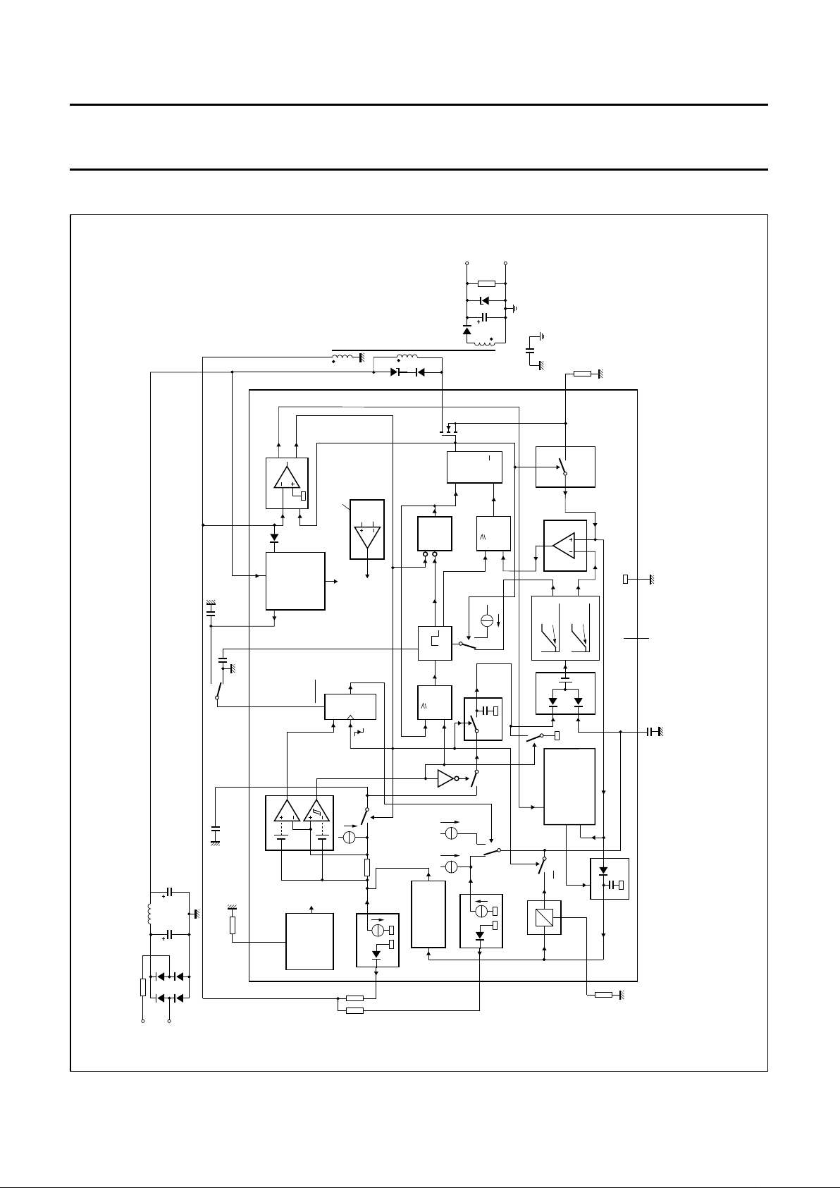
BLOCK DIAGRAM
handbook, full pagewidth
MBH570
11
BAND-GAP
TEA1401T
VOLTAGE SETTING
R
OUT
COMPENSATION
low voltage
over voltage
I
ref
G
OUT
COMPENSATION
1/6
G
OUT
7
R
I
12
R
V
T1
auxiliary
winding
V
I
J
ref
J
ref
J
ref/3
1
1
D
RESET
maximum
on time
TEMPERATURE
PROTECTION
POR
SUPPLY
TIMING
FET turn-off
V
in
from mains rectifier and filter
117V
in
14313
V
IC
C
PFM
FOLDBACK
10
C
V
9
mains
hard wired
R
ref
V
gap
V
AT
secondary
stroke
T1
primary
winding
T1
secondary
winding
C
y
SINGLE-SHOT
D-TYPE
FLIP-FLOP
foldback
clock
TR
I
TOP
REGULATOR
LEADING EDGE
BLANKING
20
TP
25 µA
I
U
8 2, 18, 19 5, 6, 15, 16
n.c. GND
C
I
S
R
Q
Q
DRAIN
output
4 SOURCE
on
Q
&
temp
max
over
temperature
MINIMUM
TRACK-
AND-
HOLD
PEAK
DETECTOR
I
PEAK
CORRECTION
CURRENT
SETTING
LIMITER
out
130 µA
2.5 µA
in
out
1.2 V
90 mV
in
R
I
I
g
m
=
Fig.1 Block diagram.
1997 Mar 07 4
Philips Semiconductors Preliminary specification
Power plug for the universal mains TEA1401T
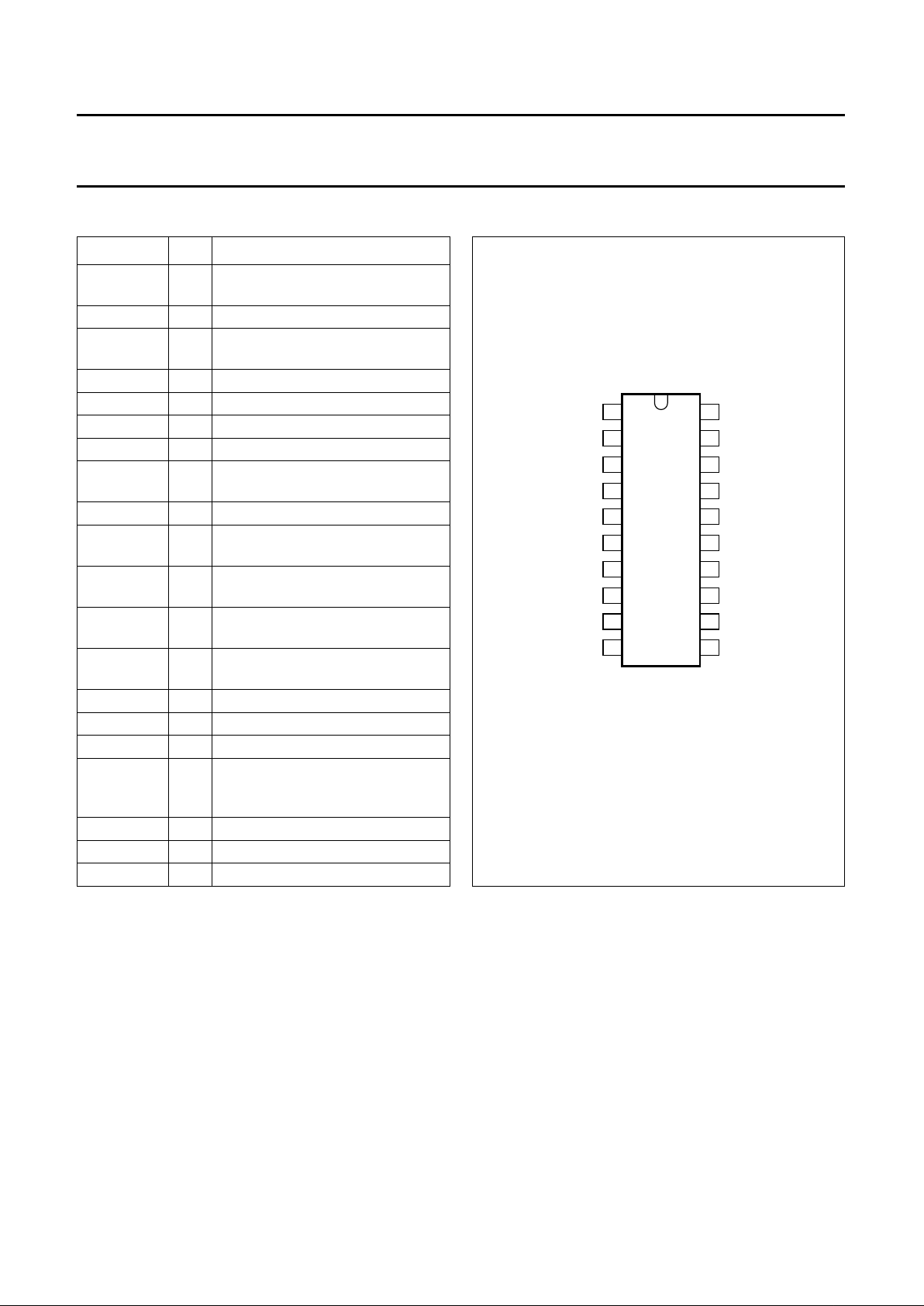
PINNING
SYMBOL PIN DESCRIPTION
V
in
1 input for rectified and filtered mains
voltage for initial powering
n.c. 2 not connected
C
PFM
3 frequency range setting for the
pulse frequency modulation
SOURCE 4 source of internal MOS switch
GND1 5 ground 1
GND2 6 ground 2
R
I
7 setting of nominal output current
C
I
8 frequency compensation of
current control loop
R
ref
9 setting of reference current
C
V
10 frequency compensation of voltage
control loop
G
OUT
11 nulling of the output conductance
of the current source function
R
V
12 setting of the nominal output
voltage
FOLDBACK 13 enabling of the foldback feature in
the output characteristic
V
IC
14 buffering of internal supply voltage
GND3 15 ground 3
GND4 16 ground 4
V
AT
17 input for voltage and power from
auxiliary winding for timing and
powering
n.c. 18 not connected
n.c. 19 not connected
DRAIN 20 drain of internal MOS switch
Fig.2 Pin configuration.
handbook, halfpage
TEA1401T
MBH571
1
2
3
4
5
6
7
8
9
10
20
19
18
17
16
15
14
13
12
11
V
in
C
PFM
R
I
C
I
R
ref
C
V
SOURCE
GND1
GND2
n.c.
DRAIN
GND4
n.c.
n.c.
V
AT
GND3
FOLDBACK
V
IC
R
V
G
OUT

1997 Mar 07 5
Philips Semiconductors Preliminary specification
Power plug for the universal mains TEA1401T
FUNCTIONAL DESCRIPTION
The TEA1401T is the heart of a compact flyback DC-to-DC
converter, with the IC placed at the primary side.
An auxiliary primary winding of the transformer is used for
indirect feedback to control the isolated output. This extra
winding also powers the device.
Control of the converted power is carried out by current
mode control and Pulse Frequency Modulation (PFM), as
illustrated in Fig.1. The primary current is sensed by a
comparator. The frequency is determined by the maximum
of the transformer demagnetizing time and the time of the
voltage controlled monostable multivibrator (single-shot).
The TEA1401T senses signals at the primary side of the
transformer to reconstruct the current and voltage which
are present at the secondary side. Comparison of these
reconstructions with the internal reference leads to
adaptation of the turn-off current level for the primary
switch and also to adaptation of the single-shot time.
Current control (see Fig.3)
The current through the main switch is measured by the
peak detector shown in Fig.1. The timing block generates
a signal ‘secondary stroke’ which is logic 1 when the
voltage of the auxiliary winding is negative.
The measured peak current, multiplied by the ratio of the
resistors connected to pins 4 (SOURCE) and 7 (R
I
), is
integrated by a capacitor during the secondary stroke.
In this way a reconstruction is made of the secondary
charge transfer. The charge estimation Q-pulse’
(see Fig.3) is drawn from the capacitor at pin 8 (CI) for
each pulse. Also this capacitor, the charge error memory,
is continuously charged with the reference current. In this
way the real (reconstructed) current is compared with the
reference yielding the voltage VCI at pin 8. The VCI level
provides the turn-off current level for the main switch and
the single-shot time.
Input from the voltage part of the loop is used to improve
the current reconstruction, resulting in a lower output
conductance of the complete converter. In the block
diagram this is denoted as ‘G
OUT
compensation’.
The block ‘I
PEAK
correction’ is able to increase the output
from the peak detector to improve line regulation.
Voltage control
The voltage from the auxiliary winding is sensed as a
measure of the secondary voltage. During the secondary
stroke the auxiliary winding delivers a negative voltage.
This voltage is converted into a current by an external
resistor at the R
V
pin between the transformer winding and
virtual ground. This current is compared with a reference
current.
The difference between the reconstructed voltage and the
reference is integrated during the secondary stroke by a
capacitor on the C
V
pin. The voltage on the CV pin is
transferred, via a ‘track-and-hold’ circuit, to the connection
point of the current and the voltage loop.
The ‘track-and-hold’ output provides the turn-off current
level for the main switch and the single-shot time.
The ‘track-and-hold’ circuit itself is present for loop
stability.
Input from the current part of the loop is used to improve
the voltage reconstruction, resulting in lower output
impedance of the complete converter (analog to the
current control). In the block diagram this is denoted as
‘R
OUT
compensation’.
Combined control
The two loops, I loop and V loop, each request their own
turn-off current level for the main switch and single-shot
time. The block ‘minimum’ in the block diagram outputs the
lowest value of the two, preventing the output voltage or
current from exceeding its nominal value. The output
characteristics of the power plug are displayed in Fig.4
(with enabled foldback option).
Optional foldback (see Fig.4)
The optional foldback feature of the TEA1401T is
performed by sensing the voltage of the auxiliary winding
at the end of the flyback stroke. It is actually not a voltage,
but the current through pin 12 (RV) that is measured. When
this voltage is low, the reference current in the current
control loop is set to the low level J
ref
/3.
The steep foldback enables a turn-down of the converter
by short-circuiting the output on the secondary side, for
example by a switch-transistor.

1997 Mar 07 6
Philips Semiconductors Preliminary specification
Power plug for the universal mains TEA1401T
Overshoot protection
Sensing the voltage during the previously mentioned
flyback stroke is also used to signal a voltage overshoot.
A voltage overshoot will delay and minimize the next active
stroke. This is achieved by discharging the capacitor in the
‘track-and-hold’ circuit (see Fig.1). In this way the power
level of the converter is turned down to its minimum
immediately in case of a voltage overshoot.
Minimum output power
Under no-load condition an additional external pre-load
resistor (or Zener diode) is necessary to keep the output
voltage at its nominal value (or at the Zener diode voltage).
This is due to the fact that under no-load condition and also
at voltage overshoot the converter will keep operating
instead of being switched off. Although the converter then
will operate with a short active stroke and a low frequency,
energy is still being converted to the output. To prevent
excessive output voltage this energy has to be dissipated.
The advantage of a pre-load resistor over a Zener diode is
that the converter will stay in regulation, maintaining its fast
response to load variations.
Duty cycle control
The momentary power level required by the I/V control
loop is achieved by controlling the duty cycle of the
converter by two actions. First the peak value of the
primary current is controlled using a cycle-by-cycle current
control. Secondly the pulse frequency is modulated. There
is a broad region in which both regulation principles are
active simultaneously. Both controls have a minimum and
a maximum value which are set by the resistor on the
SOURCE pin and the capacitor on the C
PFM
pin.
SOPS and PFM
The switching frequency f
sw
is set by the transformer
demagnetizing time or the frequency control block within
the IC (block ‘single-shot’ in Fig.1).
At a high power level the transformer determines the
frequency. This mode of operation is called Self Oscillating
Power Supply (SOPS), and provides maximum efficiency
(for a non-continuous conducting flyback converter).
In SOPS the next primary stroke is started right after the
previous secondary stroke has ended. Timing information
is collected from the auxiliary winding.
The SOPS frequency will increase when the power level
decreases. The frequency however is limited by the PFM
controller (single-shot). When the PFM controller takes
over, the frequency will be proportional to the required
power level. Thus the frequency is reduced when the
power level decreases. In PFM there is a variable dead
time after the secondary stroke. The next primary stroke is
started after the single-shot time has ended.
Supply
Initially the IC is powered by a high DC input voltage at
pin 1 (V
in
). In operation the auxiliary winding takes over.
In the event that the auxiliary winding delivers insufficient
power for the internal circuitry of the IC, this deficit is
supplemented again via pin 1 (Vin).
The supply voltage for the internal circuitry is buffered with
an external capacitor at pin 14 (VIC). When the auxiliary
winding powers the IC, energy is stored during the active
stroke. The rest of the time energy is supplied by the buffer
capacitor.
Protections
The IC has a cycle-by-cycle current regulation, with a
built-in setting for the absolute maximum voltage across
the current sense resistor. Also a maximum time is set for
the duration of the active stroke. A provision for
temperature shut down has been implemented.
 Loading...