


INTEGRATED CIRCUITS
DATA SH EET
TDA8787A
10-bit, 3.0 V, up to 25 Msps
analog-to-digital interface for CCD
cameras
Product specification
Supersedes data of 2000 Oct 12
File under Integrated Circuits, IC02
2000 Nov 14

Philips Semiconductors Product specification
10-bit, 3.0 V, up to 25 Msps analog-to-digital
interface for CCD cameras
FEATURES
• Correlated Double Sampling (CDS), Programmable
GainAmplifier (PGA),10-bitAnalog-to-DigitalConverter
(ADC) and reference regulator included
• Fully programmable via a 3-wire serial interface
• Sampling frequency up to 25 MHz;
(TDA8787AHL = 18 MHz; TDA8787AHL/S1 = 25 MHz)
• PGA gain range of 36 dB (in steps of 0.1 dB)
• Low power consumption of only 170 mW at 2.7 V
• Power consumption in standby mode of 4.5 mW
(typical value)
• 3.0 V operation; 2.5 to 3.6 V operation for the digital
outputs
• Active control pulses polarity selectable via serial
interface
• 8-bit DAC included for analog settings
• TTL compatible inputs, CMOS compatible outputs.
APPLICATIONS
• Low-power, low-voltage CCD camera systems.
GENERAL DESCRIPTION
The TDA8787A is a 10-bit analog-to-digital interface for
CCD cameras. The device includes a correlated double
sampling circuit, a PGA, clamp loops and a low-power
10-bit ADC, together with its reference voltage regulator.
The PGA gain and the ADC input clamp level are
controlled via the serial interface.
An additional DAC is provided for additional system
controls. Its output voltage range is 1.0 V peak-to-peak
which is available at pin OFDOUT.
TDA8787A
ORDERING INFORMATION
PACKAGE
TYPE NUMBER
TDA8787AHL LQFP48 plastic low profile quad flat package; 48 leads;
TDA8787AHL/S1 LQFP48 SOT313-2 25 MHz
NAME DESCRIPTION VERSION
SOT313-2 18 MHz
body 7 × 7 × 1.4 mm
PIXEL
FREQUENCY
2000 Nov 14 2
Philips Semiconductors Product specification
10-bit, 3.0 V, up to 25 Msps analog-to-digital
TDA8787A
interface for CCD cameras
QUICK REFERENCE DATA
SYMBOL PARAMETER CONDITIONS MIN. TYP. MAX. UNIT
V
CCA
V
CCD
V
CCO
I
CCA
I
CCD
I
CCO
ADC
res
V
i(CDS)(p-p)
f
pix(max)
f
pix(min)
DR
PGA
N
tot(rms)
V
n(i)(eq)(rms)
P
tot
analog supply voltage 2.7 3.0 3.6 V
digital supply voltage 2.7 3.0 3.6 V
digital outputs stages supply
2.5 2.6 3.6 V
voltage
analog supply current all clamps active; f
digital supply current f
digital outputs supply current f
=18MHz − 13 17 mA
pix
= 18 MHz; CL= 20 pF; input ramp
pix
= 18 MHz − 50 60 mA
pix
− 12mA
response time is 800 µs
ADC resolution − 10 − bits
CDS input amplitude (video
signal) (peak-to-peak value)
VCC= 2.85 V 650 −−mV
≥ 3.0 V 800 −−mV
V
CC
maximum pixel frequency 25 −−MHz
minimum pixel frequency 2 −−MHz
PGA dynamic range − 36 − dB
total noise (RMS value) at
PGA code = 0; see Fig.8 − 0.15 − LSB
CDS input to ADC output
equivalent input noise
PGA code = 383 − 70 −µV
voltage (RMS value)
total power consumption V
CCA=VCCD=VCCO
V
CCA=VCCD=VCCO
=3V − 190 − mW
= 2.7 V − 170 − mW
2000 Nov 14 3
This text is here in white to force landscape pages to be rotated correctly when browsing through the pdf in the Acrobat reader.This text is here in
d
_white to force landscape pages to be rotated correctly when browsing through the pdf in the Acrobat reader.This text is here inThis text is here in
white to force landscape pages to be rotated correctly when browsing through the pdf in the Acrobat reader. white to force landscape pages to be ...
2000 Nov 14 4
book, full pagewidth
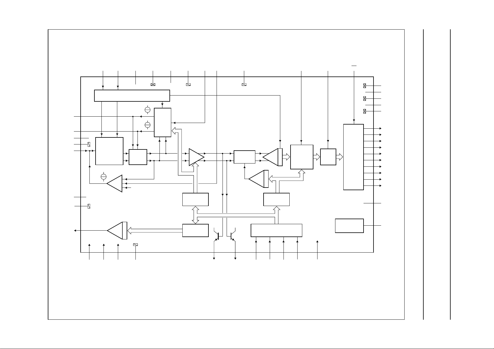
BLOCK DIAGRAM
Philips Semiconductors Product specification
10-bit, 3.0 V, up to 25 Msps analog-to-digital
interface for CCD cameras
CPCDS1
CPCDS2
V
CCA3
AGND3
V
CCA1
AGND1
OFDOUT
V
SHP
SHD
47
CDS CLOCK GENERATOR
7
8
42
41
CORRELATED
4
IN
6
5
9
DOUBLE
SAMPLING
input
clamp
OFD DAC
CCD3
1
48
V
ref
DGND3
2
V
CLAMP
CCA2
AGND2
18
17
PGA
9-BIT
REGISTER
8-BIT
REGISTER
CLPOB
13
CLPDM
12
AGND5
43
TDA8787AHL
SHIFTERSHIFT
DAC
10-bit ADC
REGISTER
SERIAL
INTERFACE
7-BIT
BLK
11
BLANKING
CLK
LATCH
40
REGULATOR
OE
37
OUTPUT
BUFFER
20
DGND1
19
V
CCD1
39
DGND2
38
V
CCD2
26
OGND
36
D9
35
D8
34
D7
33
D6
32
D5
31
D4
30
D3
29
D2
28
D1
27
D0
25
V
CCO
44
DCLPC
15
14 3
TEST2
TEST1 AGND4
16
TEST3
45
OPGA OPGAC
46
Fig.1 Block diagram.
SEN
22
23
SCLK
SDATA
21
24
VSYNC
10
FCE330
STDBY
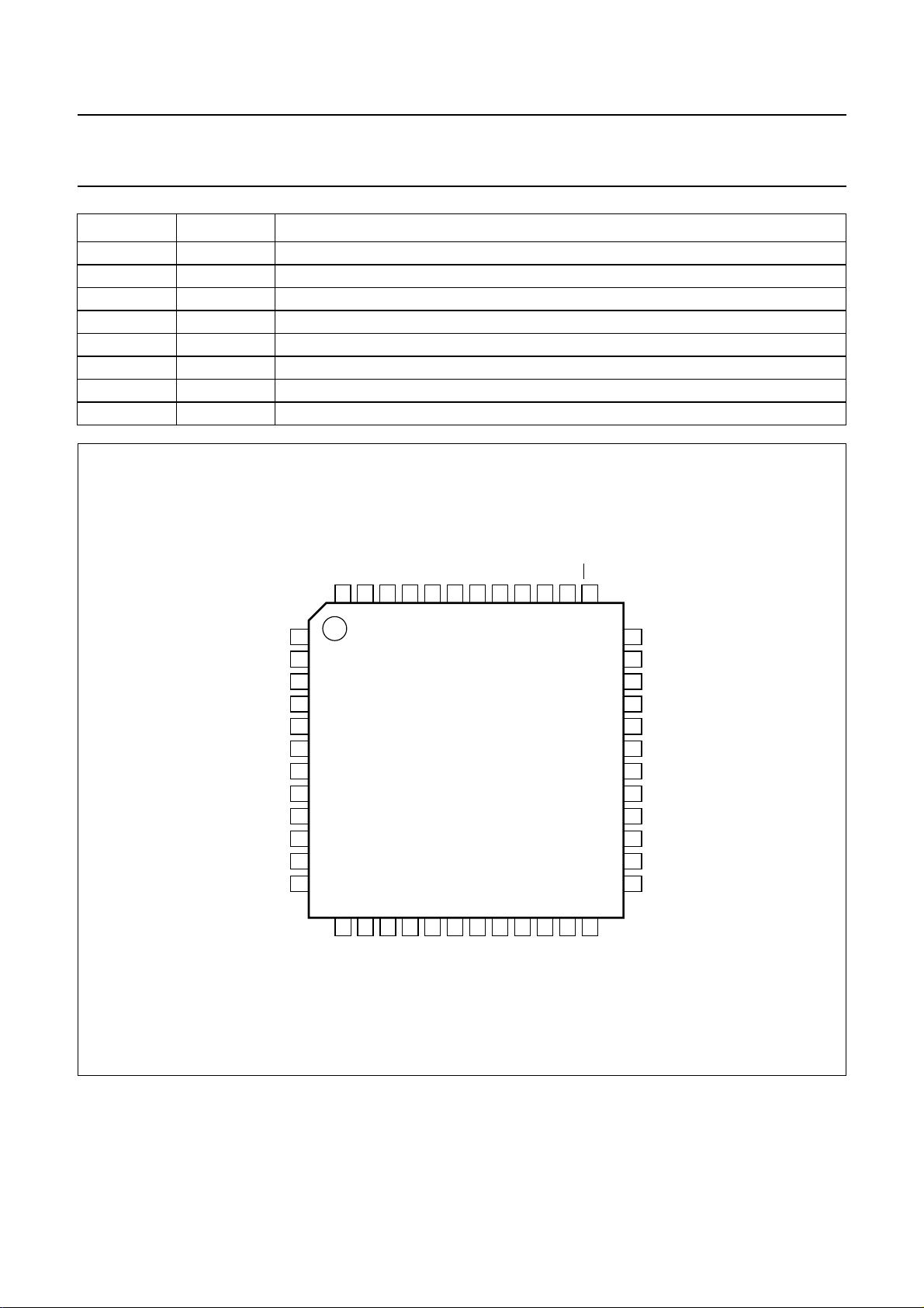
TDA8787A
Philips Semiconductors Product specification
10-bit, 3.0 V, up to 25 Msps analog-to-digital
TDA8787A
interface for CCD cameras
PINNING
SYMBOL PIN DESCRIPTION
V
CCD3
DGND3 2 digital ground 3
AGND4 3 analog ground 4
IN 4 input signal from CCD
AGND1 5 analog ground 1
V
CCA1
CPCDS1 7 clamp storage capacitor 1
CPCDS2 8 clamp storage capacitor 2
OFDOUT 9 analog output of the additional 8-bit control DAC
STDBY 10 standby mode control input (LOW: TDA8787A active; HIGH: TDA8787A standby)
BLK 11 blanking control input
CLPDM 12 clamp pulse input at dummy pixel (should be connected to ground)
CLPOB 13 clamp pulse input for optical black
TEST1 14 test pin input 1 (should be connected to AGND2)
TEST2 15 test pin input 2 (should be connected to AGND2)
TEST3 16 test pin input 3 (should be connected to AGND2)
AGND2 17 analog ground 2
V
CCA2
V
CCD1
DGND1 20 digital ground 1
SDATA 21 serial data input for serial interface control
SCLK 22 serial clock input for serial interface control
SEN 23 strobe pin for serial interface control
VSYNC 24 vertical sync pulse input
V
CCO
OGND 26 digital output ground
D0 27 ADC digital output 0 (LSB)
D1 28 ADC digital output 1
D2 29 ADC digital output 2
D3 30 ADC digital output 3
D4 31 ADC digital output 4
D5 32 ADC digital output 5
D6 33 ADC digital output 6
D7 34 ADC digital output 7
D8 35 ADC digital output 8
D9 36 ADC digital output 9 (MSB)
OE 37 output enable control input (LOW: outputs active; HIGH: outputs in high impedance)
V
CCD2
DGND2 39 digital ground 2
CLK 40 data clock input
1 digital supply voltage 3
6 analog supply voltage 1
18 analog supply voltage 2
19 digital supply voltage 1
25 output stages supply voltage
38 digital supply 2
2000 Nov 14 5
Philips Semiconductors Product specification
10-bit, 3.0 V, up to 25 Msps analog-to-digital
interface for CCD cameras
SYMBOL PIN DESCRIPTION
AGND3 41 analog ground 3
V
CCA3
AGND5 43 analog ground 5
DCLPC 44 regulator decoupling pin
OPGA 45 PGA output (test pin)
OPGAC 46 PGA complementary output (test pin)
SHP 47 preset sample-and-hold pulse input
SHD 48 data sample-and-hold pulse input
42 analog supply 3
SHD
SHP
48
47
OPGA
OPGAC
46
45
DCLPC
AGND5
44
43
CCA3
V
42
AGND3
CLK
41
40
DGND2
V
39
38
CCD2
TDA8787A
OE
37
V
CCD3
DGND3
AGND4
AGND1
V
CCA1
CPCDS1
CPCDS2
OFDOUT
STDBY
BLK
CLPDM
24
VSYNC
36
35
34
33
32
31
30
29
28
27
26
25
FCE331
D9
D8
D7
D6
D5
D4
D3
D2
D1
D0
OGND
V
CCO
1
2
3
4
IN
5
6
7
8
9
10
11
12
13
14
TEST1
CLPOB
15
TEST2
16
TEST3
TDA8787AHL
17
18
19
CCA2
CCD1
V
V
AGND2
20
21
SDATA
DGND1
22
SCLK
23
SEN
Fig.2 Pin configuration.
2000 Nov 14 6
Philips Semiconductors Product specification
10-bit, 3.0 V, up to 25 Msps analog-to-digital
TDA8787A
interface for CCD cameras
LIMITING VALUES
In accordance with the Absolute Maximum Rating System (IEC 60134).
SYMBOL PARAMETER CONDITIONS MIN. MAX. UNIT
V
CCA
V
CCD
V
CCO
∆V
CC
V
i
I
o
T
stg
T
amb
T
j
Note
1. The supply voltages V
voltage difference ∆VCC remains as indicated.
analog supply voltage note 1 −0.3 +5.0 V
digital supply voltage note 1 −0.3 +5.0 V
output stages supply voltage note 1 −0.3 +5.0 V
supply voltage difference
between V
between V
between V
CCA
CCA
CCD
and V
and V
and V
CCD
CCO
CCO
−0.5 +0.5 V
−0.5 +1.2 V
−0.5 +1.2 V
input voltage referenced to AGND −0.3 +5.0 V
data output current −±10 mA
storage temperature −55 +150 °C
ambient temperature −20 +75 °C
junction temperature − 150 °C
, V
CCA
CCD
and V
may have any value between −0.3 and +5.0 V provided that the supply
CCO
HANDLING
Inputs and outputs are protected against electrostatic discharges in normal handling. However, to be totally safe, it is
desirable to take normal precautions appropriate to handling integrated circuits.
THERMAL CHARACTERISTICS
SYMBOL PARAMETER CONDITIONS VALUE UNIT
R
th(j-a)
thermal resistance from junction to ambient in free air 76 K/W
2000 Nov 14 7
Philips Semiconductors Product specification
10-bit, 3.0 V, up to 25 Msps analog-to-digital
TDA8787A
interface for CCD cameras
CHARACTERISTICS
V
CCA=VCCD
SYMBOL PARAMETER CONDITIONS MIN. TYP. MAX. UNIT
Supplies
V
CCA
V
CCD
V
CCO
I
CCA
I
CCD
I
CCO
P
tot
Digital inputs
INPUTS: PINS STDBY, CLPDM, CLPOB, SCLK, SDATA, SEN, VSYNC, OE, CLK AND BLK
V
IL
V
IH
I
i
INPUTS: PINS SHP AND SHD
V
IL
V
IH
I
i
Clamps
= 3.0 V; V
CCO
= 2.6 V; f
= 18 MHz; T
pix
= −20 to +75°C; unless otherwise specified.
amb
analog supply voltage 2.7 3.0 3.6 V
digital supply voltage 2.7 3.0 3.6 V
digital outputs stages
2.5 2.6 3.6 V
supply voltage
analog supply current all clamps active − 50 60 mA
digital supply current − 13 17 mA
digital outputs supply
current
CL= 20 pFon all dataoutputs;
input ramp response time is
− 12mA
800 µs
total power consumption V
CCA=VCCD=VCCO
V
CCA=VCCD=VCCO
=3V − 190 − mW
= 2.7 V − 170 − mW
LOW-level input voltage 0 − 0.6 V
HIGH-level input voltage 2.2 − 5.0 V
input current 0 ≤ Vi≤ V
CCD
−2 − +2 µA
LOW-level input voltage 0 − 0.6 V
HIGH-level input voltage 2.2 − 5.0 V
input current 0 ≤ Vi≤ V
CCD
−10 − +10 µA
GLOBAL CHARACTERISTICS OF THE CLAMP LOOPS
t
W(clamp)
clamp active pulse width
in numbers of pixels
PGA input code = 255 for
maximum 4 LSB error
INPUT CLAMP: PIN CLPDM
g
m(CDS)
CDS input clamp
transconductance
OPTICAL BLACK CLAMP: PIN CLPOB
G
shift
gain from CPCDS1 and 2
to PGA inputs
I
LSB(cp)
charge pump current for
±1 LSB error at ADC
PGA input code = 0 −±20 −µA
PGA input code = 383 −±0.60 −µA
output
2000 Nov 14 8
12 −−pixels
1.5 2.7 3.5 mS
− 0.27 −
 Loading...