

Philips TDA8785H Datasheet

INTEGRATED CIRCUITS
DATA SH EET
TDA8785
8-bit high-speed analog-to-digital
converter with gain and offset
controls
Preliminary specification
File under Integrated Circuits, IC02
1996 Jan 17
Philips Semiconductors Preliminary specification
8-bit high-speed analog-to-digital
converter with gain and offset controls
FEATURES
• 8-bit analog-to-digital converter (ADC)
• 8-bit digital-to-analog converter (DAC)
• Sampling rate up to 30 Msps for both ADC and DAC
• Binary or two’s complement 3-state TTL outputs
• TTL compatible inputs and outputs
• 100 MHz variable gain amplifier (0 to 20 dB) externally
controlled
• All analog inputs and outputs are differential (can also
be used in single-ended format)
• Analog input signal from 0.1 to 1.0 V (p-p) differential
• Offset amplifier with:
– slow offset control (±250 mV)
– fast offset control (±500 mV) eventually driven by
internal DAC
• ADC output code of 8 (typ.) when analog input signal
and offset correction inputs are 0 V
TDA8785
• Gain, slow offset control inputs and DAC output swing of
1.5 V (p-p) range (2.75 ±0.75 V)
• 2.75 V reference voltage
• Internal references for ADC and DAC.
GENERAL DESCRIPTION
The TDA8785 is an 8-bit analog-to-digital converter with
gain and offset controls for the input signal. An internal
8-bit DAC provides digital adjustment of the different input
offsets.
APPLICA TIONS
• CCD type of systems
• Scanner
• Copier
• Video acquisition.
QUICK REFERENCE DATA
SYMBOL PARAMETER CONDITIONS MIN. TYP. MAX. UNIT
V
V
V
V
I
CCA
I
CCD
I
CCO
CCA1
CCA2
CCD
CCO
analog supply voltage 1 4.75 5.0 5.25 V
analog supply voltage 2 4.75 5.0 5.25 V
digital supply voltage 4.75 5.0 5.25 V
TTL output supply voltage 4.75 5.0 5.25 V
analog supply current − 80 − mA
digital supply current − 30 − mA
TTL output supply current − 9 − mA
INL integral non-linearity 0 to 20 dB gain; ramp input −±0.7 tbf LSB
DNL differential non-linearity 0 to 20 dB gain; ramp input −±0.4 tbf LSB
f
clk(max)
B controlled gain amplifier
maximum clock frequency ADC and DAC 30 −−MHz
− 100 − MHz
bandwidth
P
tot
total power dissipation − 600 − mW
ORDERING INFORMATION
TYPE
NUMBER
NAME DESCRIPTION VERSION
PACKAGE
TDA8785H QFP44 plastic quad flat package; 44 leads (lead length 1.3 mm); body 10 × 10 × 1.75 mm SOT307-2
1996 Jan 17 2
Philips Semiconductors Preliminary specification
8-bit high-speed analog-to-digital converter
with gain and offset controls
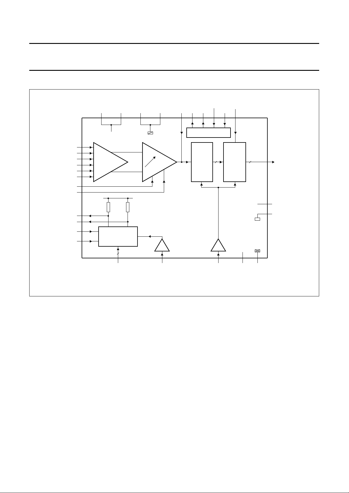
BLOCK DIAGRAM
handbook, full pagewidth
V
SOFF(p)
V
SOFF(n)
V
FOFF(p)
V
FOFF(n)
V
FSAD(p)
V
FSAD(n)
V
DACO(p)
V
DACO(n)
V
FSDAC(p)
V
FSDAC(n)
V
i(p)
V
i(n)
43
44
37
38
42
41
39
40
9
8
10
11
V
AMPLIFIER
12 to 19
AGND1
V
CCA
CCA1VCCA2
1 2 3 4
OFFSET
150 Ω 150 Ω
DAC
8
AGND2
GAIN
TDA8785
CLOCK
DRIVER
20 22
CLKDACDA7 to DA0
DEC2
V
V
B
6 7 36 5 35 34
ref
RB
REGULATORS
ADC
DEC1
8
OUTPUTS
CLOCK
DRIVER
OF
TTL
V
CCD
8
23
26 to 33
25
24
21
DGNDCLKADC
TDA8785
AD0 to AD7
V
CCO
OGND
MBG681
Fig.1 Block diagram.
1996 Jan 17 3
Philips Semiconductors Preliminary specification
8-bit high-speed analog-to-digital converter
with gain and offset controls
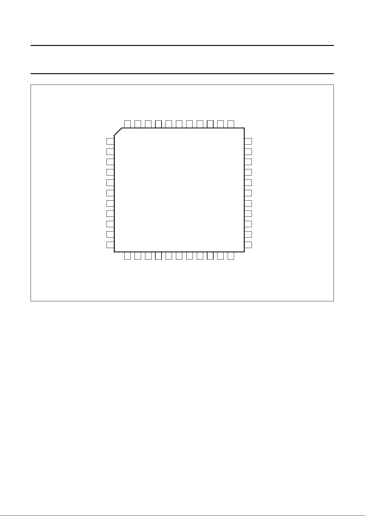
PINNING
SYMBOL PIN DESCRIPTION
V
CCA1
V
CCA2
AGND1 3 analog ground 1
AGND2 4 analog ground 2
DEC2 5 decoupling input 2
B 6 bandwidth adjustment node input
V
RB
V
DACO(n)
V
DACO(p)
V
FSDAC(p)
V
FSDAC(n)
DA7 12 DAC TTL input; bit 7 (MSB)
DA6 13 DAC TTL input; bit 6
DA5 14 DAC TTL input; bit 5
DA4 15 DAC TTL input; bit 4
DA3 16 DAC TTL input; bit 3
DA2 17 DAC TTL input; bit 2
DA1 18 DAC TTL input; bit 1
DA0 19 DAC TTL input; bit 0 (LSB)
CLKDAC 20 DAC clock input
DGND 21 digital ground
CLKADC 22 ADC clock input
V
CCD
1 analog supply voltage 1 (+5 V)
2 analog supply voltage 2 (+5 V)
7 ADC reference voltage output bottom
(decoupling)
8 DAC negative voltage output
9 DAC positive voltage output
10 DAC full-scale positive control voltage
input
11 DAC full-scale negative control
voltage input
23 digital supply voltage (+5 V)
TDA8785
SYMBOL PIN DESCRIPTION
OGND 24 output ground
V
CCO
AD0 26 output data; bit 0 (LSB)
AD1 27 output data; bit 1
AD2 28 output data; bit 2
AD3 29 output data; bit 3
AD4 30 output data; bit 4
AD5 31 output data; bit 5
AD6 32 output data; bit 6
AD7 33 output data; bit 7 (MSB)
OF 34 output format input
DEC1 35 decoupling input 1
V
ref
V
SOFF(p)
V
SOFF(n)
V
FSAD(p)
V
FSAD(n)
V
FOFF(n)
V
FOFF(p)
V
i(p)
V
i(n)
25 output supply voltage (+5 V)
36 reference voltage output (2.75 V)
37 slow offset amplifier positive voltage
input
38 slow offset amplifier negative voltage
input
39 gain control positive voltage input
40 gain control negative voltage input
41 fast offset amplifier negative voltage
input
42 fast offset amplifier positive voltage
input
43 analog positive voltage input
44 analog negative voltage input
1996 Jan 17 4
Philips Semiconductors Preliminary specification
8-bit high-speed analog-to-digital converter
with gain and offset controls
handbook, full pagewidth
SOFF(n)
FSAD(p)
FSAD(n)
FOFF(n)
FOFF(p)
i(p)
V
CCA1
V
CCA2
AGND1
AGND2
DEC2
V
DACO(n)
V
DACO(p)
V
FSDAC(p)
V
FSDAC(n)
i(n)
V
44
1
2
3
4
5
B
6
V
7
RB
8
9
10
11
V
V
43
42
V
41
V
40
TDA8785
V
V
39
38
SOFF(p)
V
V
37
36
ref
DEC1
35
OF
34
TDA8785
33
AD7
32
AD6
31
AD5
AD4
30
AD3
29
28
AD2
AD1
27
AD0
26
V
25
CCO
OGND
24
V
23
CCD
12
DA7
13
14
15
16
17
DA6
DA5
DA4
DA3
DA2
Fig.2 Pin configuration.
18
DA1
19
DA0
20
21
DGND
CLKDAC
MBG680
22
CLKADC
1996 Jan 17 5

Philips Semiconductors Preliminary specification
8-bit high-speed analog-to-digital converter
with gain and offset controls
FUNCTIONAL DESCRIPTION
The TDA8785 is composed of an 8-bit ADC (30 Msps), a
wide-band gain amplifier, an input offset amplifier and an
8-bit dynamic adjustment DAC.
Input signal
Two input pins are provided to apply a differential input
signal with a wide range (100 to 1000 mV differential). It is
also possible to apply a single signal by setting a DC
voltage on one of the differential pins and supplying the
signal to the other.
Controlled gain amplifier
The gain amplifier is used to adjust the wide input signal
range to the fixed ADC input range of 1 V (p-p).
A large gain of 20 dB can be achieved with low-noise
behaviour and a large bandwidth of 100 MHz to correctly
amplify square type signals with step edges. Using pin 6,
it is possible to reduce the internal bandwidth of the gain
amplifier via an external capacitor and thus improve its
noise behaviour. The gain amplifier is controlled via an
external differential voltage (single input can also be
applied).
TDA8785
The internal 8-bit DAC operates at the ADC clock rate to
allow dynamic corrections on the input signal chain based
on the signal processing information carried out after the
digital conversion. The output voltage amplitude of the
DAC can be controlled via a different input voltage (which
can also be single) in a range of ±25% with a 150 Ω DAC
output load.
The DAC can also be used for the gain or the slow offset
control with some external DC voltage adaptations and
can be considered as a separate function of the ADC
chain. The DAC can be used independently, for example
as a video DAC.
8-bit ADC
The 8-bit ADC converts a signal of 1 V (p-p) from the
controlled gain amplifier into an 8-bit coded digital word at
a maximum rate of 30 Msps. Its reference voltage is
supplied by the general voltage regulator. The output data
format can either be binary, two’s complement or 3-state
by selecting pin OF.
When all the differential inputs on the offset amplifier
(V
0 V (equivalent to both inputs short-circuited), the output
code of the ADC is code 8.
SOFF(p)
, V
SOFF(n)
, V
FOFF(n)
, V
FOFF(p)
, V
i(p)
and V
) are at
i(n)
Input offset amplifier and adjustment DAC
The Input offset amplifier contains two different control
inputs (which can also be single):
• Slow offset control, for slow variation characteristics
(e.g. temperature, supply voltage, etc.)
• Fast offset control, for correction related to the clock
rate.
Slow offset control is carried out by an external voltage
while fast offset control is digitally carried out via the
internal 8-bit DAC with external connections of the
respective pins V
DACO(n)
, V
DACO(p)
, V
FOFF(n)
and V
FOFF(p)
Internal voltage regulator
An internal voltage regulator provides all the references for
the different blocks. A stable 2.75 V voltage reference
output is provided for use in the application environment.
One application is to connect all the slow control inputs
(V
FSDAC(p)
V
FSAD(n)
, V
FSDAC(n)
) to this reference, either to their two differential
, V
SOFF(p)
, V
SOFF(n)
, V
FSAD(p)
inputs to get the nominal settings or to one of the
differential inputs to have easy single-input control.
All these control inputs have the same control range.
.
and
1996 Jan 17 6
Philips Semiconductors Preliminary specification
8-bit high-speed analog-to-digital converter
TDA8785
with gain and offset controls
LIMITING VALUES
In accordance with the Absolute Maximum Rating System (IEC 134).
SYMBOL PARAMETER CONDITIONS MIN. MAX. UNIT
V
CCA
V
CCD
V
CCO
∆V
CC
V
I
V
clk(p-p)
I
O
T
stg
T
amb
T
j
analog supply voltage −0.3 +7.0 V
digital supply voltage −0.3 +7.0 V
output supply voltage −0.3 +7.0 V
supply voltage difference between
V
V
V
CCA
CCD
CCA
and V
and V
and V
CCD
CCO
CCO
−1.0 +1.0 V
−1.0 +1.0 V
−1.0 +1.0 V
input voltage referenced to AGND −0.3 +7.0 V
clock input voltage for switching (peak-to-peak value) referenced to DGND − V
CCD
V
output current − 6mA
storage temperature −55 +150 °C
operating ambient temperature 0 70 °C
junction temperature − 150 °C
THERMAL CHARACTERISTICS
SYMBOL PARAMETER VALUE UNIT
R
th j-a
thermal resistance from junction to ambient in free air 75 K/W
1996 Jan 17 7

Philips Semiconductors Preliminary specification
8-bit high-speed analog-to-digital converter
TDA8785
with gain and offset controls
CHARACTERISTICS
V
CCA1=VCCA2=VCCD=VCCO
V
CCA
to V
CCD=VCCD
to V
typical values measured at V
SYMBOL PARAMETER CONDITIONS MIN. TYP. MAX. UNIT
Supplies
V
V
V
V
I
CCA
I
CCD
I
CCO
CCA1
CCA2
CCD
CCO
analog supply voltage 1 4.75 5.0 5.25 V
analog supply voltage 2 4.75 5.0 5.25 V
digital supply voltage 4.75 5.0 5.25 V
TTL output supply voltage 4.75 5.0 5.25 V
analog supply current − 80 − mA
digital supply current − 30 − mA
TTL output supply current − 9 − mA
Reference voltages (pins V
V
ref
V
line
I
LO
V
RB
output reference voltage 2.60 2.75 2.90 V
line regulation voltage V
output load current −1 −−mA
reference voltage output bottom
(decoupling)
V
∆V
osB
ADC
offset voltage bottom code 0 − V
ADC reference voltage difference between code 0 and 255 − 1 − V
Analog inputs (pins V
V
i(p-p)
V
I
I
i
Z
i
C
i
differential input voltage
V
− V
i(p)
i(n)
DC input voltage − 3.0 − V
input current − 10 −µA
input impedance − 20 − kΩ
input capacitance − 1 − pF
Fast amplifier inputs (pins V
V
FOFF(p)
V
FOFF(n)
V
I
I
i
Z
i
C
i
input voltage 0 dB gain − 500 − mV
input voltage 0 dB gain − 500 − mV
DC input voltage − V
input current − 10 −µA
input impedance − 20 − kΩ
input capacitance − 1 − pF
= 4.75 to 5.25 V; AGND, DGND and OGND short-circuited together;
CCO=VCCA
CCA=VCCD=VCCO
ref
to V
and VRB)
=−0.25 to +0.25 V; T
CCO
= 5 V and T
CCA
= 0 to 70 °C;
amb
=25°C; unless otherwise specified.
amb
= 4.75 to 5.25 V − 4 − mV
− V
− 250 − mV
I(p)
and V
); see Table 1
I(n)
RB
0 dB gain − 1000 − mV
(peak-to-peak value)
and V
FOFF(p)
20 dB gain − 100 − mV
); DC parameters
FOFF(n)
20 dB gain − 50 − mV
20 dB gain − 50 − mV
− 2.5 − V
CCA
0.25 − V
CCA −
1996 Jan 17 8
 Loading...