

Philips TDA8783HL-C3, TDA8783HL-C2, TDA8783HL-C1 Datasheet

DATA SH EET
Product specification
Supersedes data of 1998 Jul 31
File under Integrated Circuits, IC02
1999 Jun 25
INTEGRATED CIRCUITS
TDA8783
40 Msps, 10-bit analog-to-digital
interface for CCD cameras

1999 Jun 25 2
Philips Semiconductors Product specification
40 Msps, 10-bit analog-to-digital interface
for CCD cameras
TDA8783
FEATURES
• Correlated Double Sampling (CDS), AGC, 10-bit ADC
and reference regulator included, adjustable bandwidth
(CDS and AGC)
• Fully programmable via a 3-wire serial interface
• Sampling frequency up to 40 MHz
• AGC gain from 4.5 to 34.5 dB (in 0.1 dB steps)
• CDS programmable bandwidth from 4 to 120 MHz
• AGC programmable bandwidth from 4 to 54 MHz
• Standby mode available for each block for power saving
applications 20 mW (typ.)
• 6 dB fixed gain analog output for analog iris control
• 8-bit and 10-bit DAC included for analog settings
• Low power consumption of only 483 mW (typ.)
• 5 V operation and 2.5 to 5.25 V operation for the digital
outputs
• TTL compatible inputs, TTL and CMOS compatible
outputs.
APPLICATIONS
• CCD camera systems.
GENERAL DESCRIPTION
The TDA8783 is a 10-bit analog-to-digital interface for
CCD cameras. The device includes a correlated double
sampling circuit, AGC and a low-power 10-bit
Analog-to-Digital Converter (ADC) together with its
reference voltage regulator.
The AGC and CDS have a bandwidth circuit controlled by
on-chip DACs via a serial interface.
A 10-bit DAC controls the ADC input clamp level.
An additional 8-bit DAC is provided for additional system
controls; its output voltage range is 1.4 V (p-p) which is
available at pin OFDOUT.
ORDERING INFORMATION
TYPE
NUMBER
PACKAGE
NAME DESCRIPTION VERSION
TDA8783HL LQFP48 plastic low profile quad flat package; 48 leads; body 7 × 7 × 1.4 mm SOT313-2
1999 Jun 25 3
Philips Semiconductors Product specification
40 Msps, 10-bit analog-to-digital interface
for CCD cameras
TDA8783
QUICK REFERENCE DATA
SYMBOL PARAMETER CONDITIONS MIN. TYP. MAX. UNIT
V
CCA
analog supply voltage 4.75 5 5.25 V
V
CCD
digital supply voltage 4.75 5 5.25 V
V
CCO
digital outputs supply voltage 2.5 3 5.25 V
I
CCA
analog supply current − 78 85 mA
I
CCD
digital supply current − 18 20 mA
I
CCO
digital outputs supply current f
CLK
= 27 MHz;
CL= 20 pF; ramp input
− 1 − mA
ADC
res
ADC resolution − 10 − bits
V
i(CDS)(p-p)
CDS input voltage (peak-to-peak value) − 400 1200 mV
G
CDS
CDS output amplifier gain − 6 − dB
f
CLK(max)
maximum clock frequency f
cut(CDS)
= 120 MHz;
f
cut(AGC)
= 54 MHz
40 −−MHz
AGC
dyn
AGC dynamic range − 30 − dB
N
tot(rms)
total noise from CDS input to ADC output
(RMS value)
gain = 4.5 dB;
f
cut(CDS)
= 120 MHz;
f
cut(AGC)
= 54 MHz
− 0.125 − LSB
P
tot
total power consumption − 483 550 mW
1999 Jun 25 4
Philips Semiconductors Product specification
40 Msps, 10-bit analog-to-digital interface
for CCD cameras
TDA8783
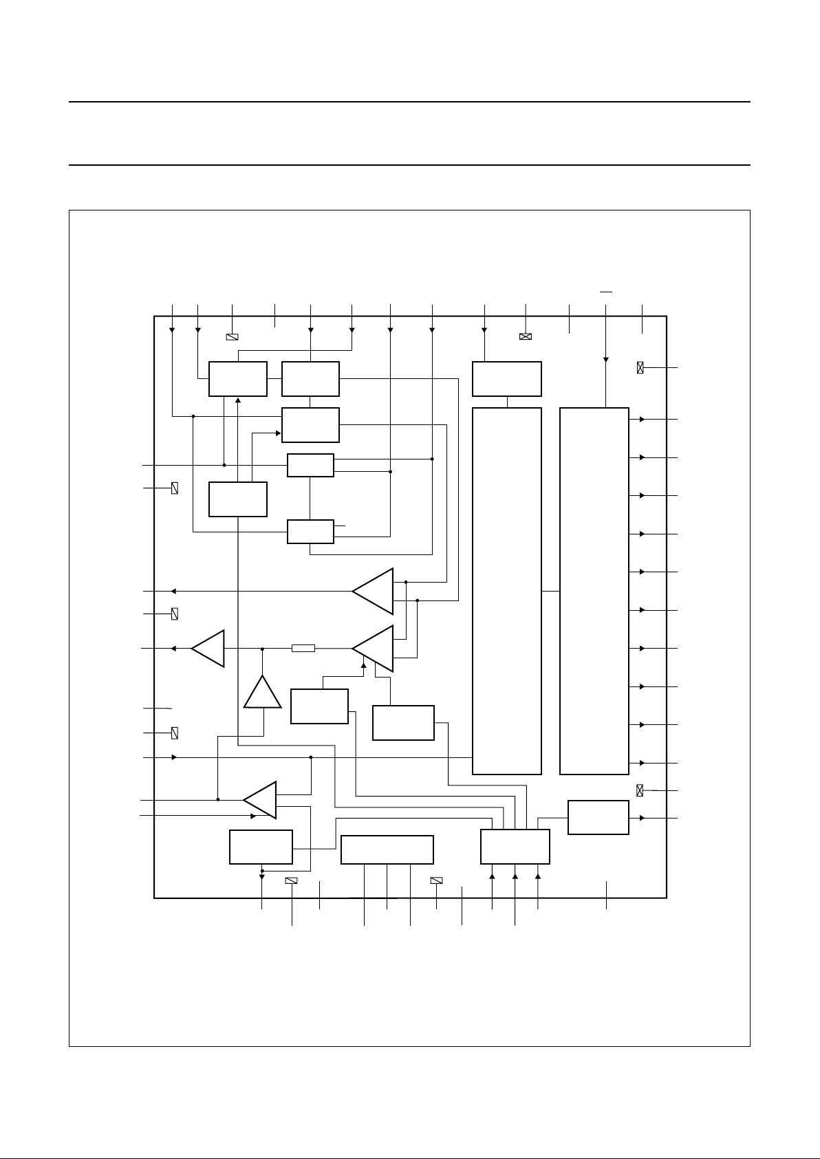
BLOCK DIAGRAM
Fig.1 Block diagram.
handbook, full pagewidth
MGM491
TRACK-
AND-HOLD
TRACK-
AND-HOLD
TRACK-
AND-HOLD
CLAMP
ref1
CLAMP
8-BIT DAC
10-BIT DAC
9-BIT DAC
6 dB
AGC
CLOCK
GENERATOR
10-BIT ADC
REGULATOR
SERIAL
INTERFACE
4-BIT DAC
CUT-OFF
OUTPUTS
BUFFER
5
4
2
7
6
9
10
14
11
12
13 15 16 17 18
20
21
22
2319
24
36
3
25
26
27
28
29
30
31
32
33
34
35
3738394041424344
454846
47
IND INP AGND3 SHD SHP CLPDM CLK
DGND2
V
CCO
V
CCD2
V
CCA3
OE
D9
D8
D7
D6
D5
D4
D3
D2
D1
D0
DGND1
OFDOUT
OGND
V
CCD1
STDBY
SENAGND6
SCLK
SDATA
DEC1
V
RT
V
RB
V
CCA2
DACOUT
V
ref
CLPADC
AGND2
ADCIN
AGND5
V
CCA1
AGCOUT
AGND4
AGND1
8
CPCDS
AMPOUT
TDA8783
4-BIT DAC
CUT-OFF
1
CLPOB
+
-
1
1
1999 Jun 25 5
Philips Semiconductors Product specification
40 Msps, 10-bit analog-to-digital interface
for CCD cameras
TDA8783
PINNING
SYMBOL PIN DESCRIPTION
CLPOB 1 clamp pulse input at optical black
AGND4 2 analog ground 4
OFDOUT 3 analog output of the additional 8-bit control DAC (controlled via the serial interface)
AMPOUT 4 CDS amplifier output (fixed gain = 6 dB)
AGND1 5 analog ground 1
V
CCA1
6 analog supply voltage 1
AGCOUT 7 AGC amplifier signal output
CPCDS 8 clamp storage capacitor pin
AGND5 9 analog ground 5
ADCIN 10 ADC analog signal input from AGCOUT via a short circuit
CLPADC 11 clamp control input for ADC analog input signal clamp (used with a capacitor from V
ref
to ground)
V
ref
12 ADC input clamp reference voltage (normally connected to pin VRB or DACOUT, or shorted to
ground via a capacitor)
DACOUT 13 DAC output for ADC clamp level
AGND2 14 analog ground 2
V
CCA2
15 analog supply voltage 2
V
RB
16 ADC reference voltage (BOTTOM) code 0
V
RT
17 ADC reference voltage (TOP) code 1023
DEC1 18 decoupling 1 (decoupled to ground via a capacitor)
AGND6 19 analog ground 6
SDATA 20 serial data input for the 4 control DACs (9-bit DAC for AGC gain, 8-bit DAC for frequency cut-off,
additional 8-bit DAC for OFD output voltage and 10-bit DAC for ADC clamp level and standby
mode per block and edge pulse control; see Table 1
SCLK 21 serial clock input for the control DACs and their serial interface; see Table 1
SEN 22 enable input for the serial interface shift register (active when SEN = logic 0); see Table 1
STDBY 23 standby control (active HIGH); all the output bits are logic 0 when standby is enabled
V
CCD1
24 digital supply voltage 1
DGND1 25 digital ground 1
D0 26 ADC digital output 0 (LSB)
D1 27 ADC digital output 1
D2 28 ADC digital output 2
D3 29 ADC digital output 3
D4 30 ADC digital output 4
D5 31 ADC digital output 5
D6 32 ADC digital output 6
D7 33 ADC digital output 7
D8 34 ADC digital output 8
D9 35 ADC digital output 9 (MSB)
OGND 36 digital output ground
V
CCO
37 digital output supply voltage
1999 Jun 25 6
Philips Semiconductors Product specification
40 Msps, 10-bit analog-to-digital interface
for CCD cameras
TDA8783
OE 38 output enable (active LOW: digital outputs active; active HIGH: digital outputs high impedance)
V
CCD2
39 digital supply voltage 2
DGND2 40 digital ground 2
CLK 41 ADC clock input
CLPDM 42 clamp pulse input at dummy pixel
SHP 43 pre-set sample-and-hold pulse input
SHD 44 data sample-and-hold pulse input
V
CCA3
45 analog supply voltage 3
INP 46 pre-set input signal from CCD
IND 47 data input signal from CCD
AGND3 48 analog ground 3
SYMBOL PIN DESCRIPTION
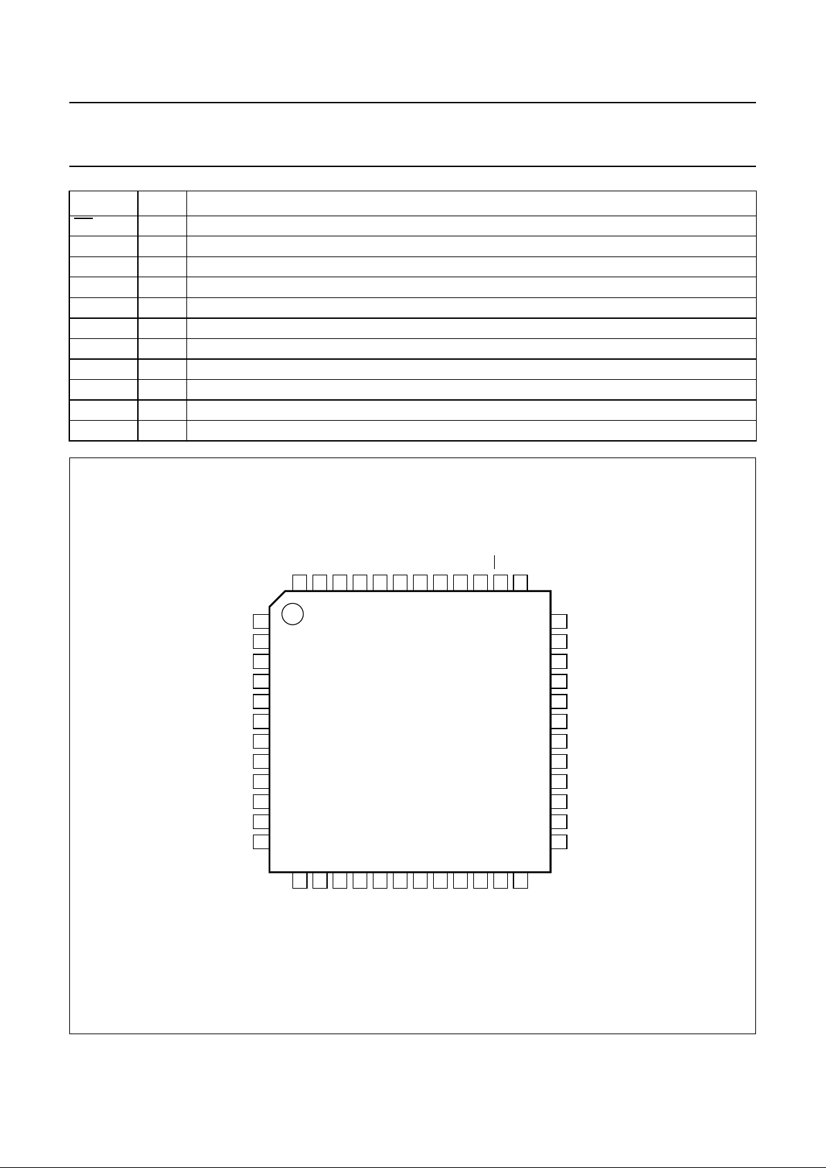
Fig.2 Pin configuration.
1
2
3
4
5
6
7
8
9
10
11
36
35
34
33
32
31
30
29
28
27
26
13
14
15
16
17
18
19
20
21
22
23
48
47
46
45
44
43
42
41
40
39
38
12
24 37
25
TDA8783H
MGM492
OGND
D9
D8
D7
D5
D4
D3
D2
D1
D0
DGND1
CLPOB
AGND4
OFDOUT
AMPOUT
AGND1
V
CCA1
CPCDS
AGND5
CLPADC
V
ref
D6
IND
INP
V
CCA3
SHD
SHP
CLPDM
DGND2
V
CCD2
OE
V
CCO
AGND3
CLK
AGCOUT
ADCIN
AGND2
V
CCA2
V
RB
V
RT
DEC1
AGND6
SDATA
SEN
STDBY
V
CCD1
DACOUT
SCLK
1999 Jun 25 7
Philips Semiconductors Product specification
40 Msps, 10-bit analog-to-digital interface
for CCD cameras
TDA8783
LIMITING VALUES
In accordance with the Absolute Maximum Rating System (IEC 134).
Note
1. The supply voltages V
CCA
, V
CCD
and V
CCO
may have any value between −0.3 and +7.0 V provided that the supply
voltage difference ∆VCC remains as indicated.
HANDLING
Inputs and outputs are protected against electrostatic discharges in normal handling. However, to be totally safe, it is
desirable to take normal precautions appropriate to handling integrated circuits.
THERMAL CHARACTERISTICS
SYMBOL PARAMETER CONDITIONS MIN. MAX. UNIT
V
CCA
analog supply voltage note 1 −0.3 +7.0 V
V
CCD
digital supply voltage note 1 −0.3 +7.0 V
V
CCO
output stages supply voltage note 1 −0.3 +7.0 V
∆V
CC
supply voltage difference
between V
CCA
and V
CCD
−1.0 +1.0 V
between V
CCA
and V
CCO
−1.0 +4.0 V
between V
CCD
and V
CCO
−1.0 +4.0 V
V
i
input voltage referenced to AGND −0.3 +7.0 V
V
CLK(p-p)
AC input voltage for switching
(peak-to-peak value)
referenced to DGND − V
CCD
V
I
o
output current − 10 mA
T
stg
storage temperature −55 +150 °C
T
amb
operating ambient temperature −20 +75 °C
T
j
junction temperature − 150 °C
SYMBOL PARAMETER CONDITIONS VALUE UNIT
R
th(j-a)
thermal resistance from junction to ambient in free air 76 K/W
1999 Jun 25 8
Philips Semiconductors Product specification
40 Msps, 10-bit analog-to-digital interface
for CCD cameras
TDA8783
CHARACTERISTICS
V
CCA=VCCD
=5V; V
CCO
=3V; f
CLK
= 27 MHz; T
amb
=25°C; unless otherwise specified.
SYMBOL PARAMETER CONDITIONS MIN. TYP. MAX. UNIT
Supplies
V
CCA
analog supply voltage 4.75 5 5.25 V
V
CCD
digital supply voltage 4.75 5 5.25 V
V
CCO
digital outputs supply voltage 2.5 3 3.6 V
I
CCA
analog supply current − 78 85 mA
I
CCD
digital supply current − 18 20 mA
I
CCO
digital outputs supply current CL= 20 pF on all data
outputs; ramp input
− 1 − mA
Digital inputs
C
LOCK INPUT: CLK (REFERENCED TO DGND)
V
IL
LOW-level input voltage 0 − 0.8 V
V
IH
HIGH-level input voltage 2.0 − V
CCD
V
I
IL
LOW-level input current V
CLK
= 0.8 V −1 − +1 µA
I
IH
HIGH-level input current V
CLK
= 2.0 V −−20 µA
Z
i
input impedance f
CLK
= 27 MHz − 46 − kΩ
C
i
input capacitance f
CLK
= 27 MHz − 1 − pF
INPUTS: SHP AND SHD
V
IL
LOW-level input voltage 0 − 0.8 V
V
IH
HIGH-level input voltage 2.0 − V
CCD
V
I
IL
LOW-level input current VIL= 0.6 V −−6−µA
I
IH
HIGH-level input current VIH= 2.2 V − 0 −µA
INPUTS: SEN, SCLK, SDATA,OE,STDBY, CLPDM, CLPOB AND CLPADC
V
IL
LOW-level input voltage 0 − 0.8 V
V
IH
HIGH-level input voltage 2.0 − V
CCD
V
I
i
input current −2 − +2 µA
Correlated Double Sampling; CDS
V
i(CDS)(p-p)
CDS input amplitude
(peak-to-peak value)
− 400 1200 mV
I
CPCDS,INP,IND
input current pins 8, 46 and 47 −2 − +2 µA
t
CDS(min)
CDS control pulses minimum
active time
f
i(CDS1,2)=fCLK(pix)
;
V
i(CDS)(p-p)
= 600 mV
black-to-white transition in
1 pixel (±1 LSB typ.);
f
cut(CDS)
= 120 MHz;
f
cut(AGC)
= 54 MHz
8 −−ns
t
hd1
hold time INP compared to control
pulse SHP
see Fig.5 − 1 − ns
t
hd2
hold time of IND compared to
control pulse SHD
see Fig.5 − 1 − ns
1999 Jun 25 9
Philips Semiconductors Product specification
40 Msps, 10-bit analog-to-digital interface
for CCD cameras
TDA8783
t
set(CDS)
CDS setting time control DAC 4 bits input
code; AGC gain = 0 dB;
f
cut(AGC)
= 54 MHz;
V
i(CDS)
= 600 mV (p-p)
black-to-white transition in
1 pixel (±1 LSB typ.)
0000 − 8 − ns
0001 − 21 − ns
0010 − 42 − ns
0011 − 52 − ns
0100 − 82 − ns
0111 − 94 − ns
1000 − 195 − ns
1011 − 219 − ns
1111 − 280 − ns
Amplifier outputs
G
AMPOUT
output amplifier gain − 6 − dB
Z
AMPOUT
output amplifier impedance − 300 −Ω
V
AMPOUT(p-p)
output amplifier dynamic voltage
(peak-to-peak value)
− 2.4 − V
V
AMPOUT(bl)
output amplifier black level
voltage
− 1.5 − V
V
AGCOUT(p-p)
AGC output amplifier dynamic
voltage level (peak-to-peak value)
− 2000 − mV
V
AGCOUT(bl)
AGC output amplifier black level
voltage
V
ref
connected to DACOUT − V
ref
− V
Z
AGCOUT(bl)
AGC output amplifier output
impedance
at 10 kHz − 5 −Ω
I
AGCOUT
AGC output static drive current static −−1mA
G
AGC(min)
minimum gain of AGC circuit AGC DAC input code = 00
(9-bit control)
− 4.5 − dB
G
AGC(max)
maximum gain of AGC circuit AGC DAC input code ≥ 319
(9-bit control)
− 34.5 − dB
f
cut(AGC)
cut-off frequency AGC 4-bit control DAC
input code = 00 − 54 − MHz
input code = 15 − 4 − MHz
Clamps
g
m(ADC)
ADC clamp transconductance at clamp level − 7 − mS
g
m(CDS)
CDS clamp transconductance at clamp level − 1.5 − mS
SYMBOL PARAMETER CONDITIONS MIN. TYP. MAX. UNIT
 Loading...