

Philips TDA8780M Datasheet

INTEGRATED CIRCUITS
DATA SH EET
TDA8780M
True logarithmic amplifier
Product specification
Supersedes data of November 1994
File under Integrated Circuits, IC03
1995 Jul 25
Philips Semiconductors Product specification
True logarithmic amplifier TDA8780M
FEATURES
• 72 dB true logarithmic dynamic range
• Small-signal gain-adjustment facility
• Constant limiting output voltage
• Temperature and DC power supply voltage independent
• Easy interfacing to analog-to-digital converters
• Output DC level shift facility.
APPLICATIONS
• Dynamic range compression
• IF signal dynamic range reduction in digital receivers
• Compression receivers.
GENERAL DESCRIPTION
The TDA8780M is a true logarithmic amplifier intended for
dynamic range reduction of IF signals at 10.7 MHz in
digital radio receivers. It offers true logarithmic
characteristics over a 72 dB input dynamic range, has a
small-signal gain-adjustment facility and a constant
limiting output voltage for large input levels.
A unique feature is the smooth “changeover” from linear
operation (inputs less than 60 µV) to logarithmic mode.
The device is manufactured in an advanced BiCMOS
process which enables high performance being obtained
with low DC power supply consumption. The true
logarithmic amplifier can be driven by single-ended or
differential inputs. The DC operating point is set by overall
on-chip feedback decoupled by two off-chip capacitors,
which define the low-frequency cut-off point.
The performance of the amplifier is stabilized against
temperature and DC power supply variations. The
differential output is converted internally to a single-ended
output by an on-chip operational amplifier arrangement in
which the DC output level is set by an externally-supplied
reference voltage. A power-down facility allows the circuit
to be disabled from a control input.
QUICK REFERENCE DATA
SYMBOL PARAMETER MIN. TYP. MAX. UNIT
V
P
I
P
I
P(PD)
f
in
V
in(M)
T
amb
supply voltage 4.5 5.0 5.5 V
supply current −−6.7 mA
supply current in power-down mode −−250 µA
operating input frequency −−15 MHz
dynamic logarithmic input voltage (peak value) 0.06 − 300 mV
operating ambient temperature −20 − +75 °C
ORDERING INFORMATION
PACKAGE
TYPE NUMBER
NAME DESCRIPTION VERSION
TDA8780M SSOP20 plastic shrink small outline package; 20 leads; body width 4.4 mm SOT266-1
1995 Jul 25 2
Philips Semiconductors Product specification
True logarithmic amplifier TDA8780M
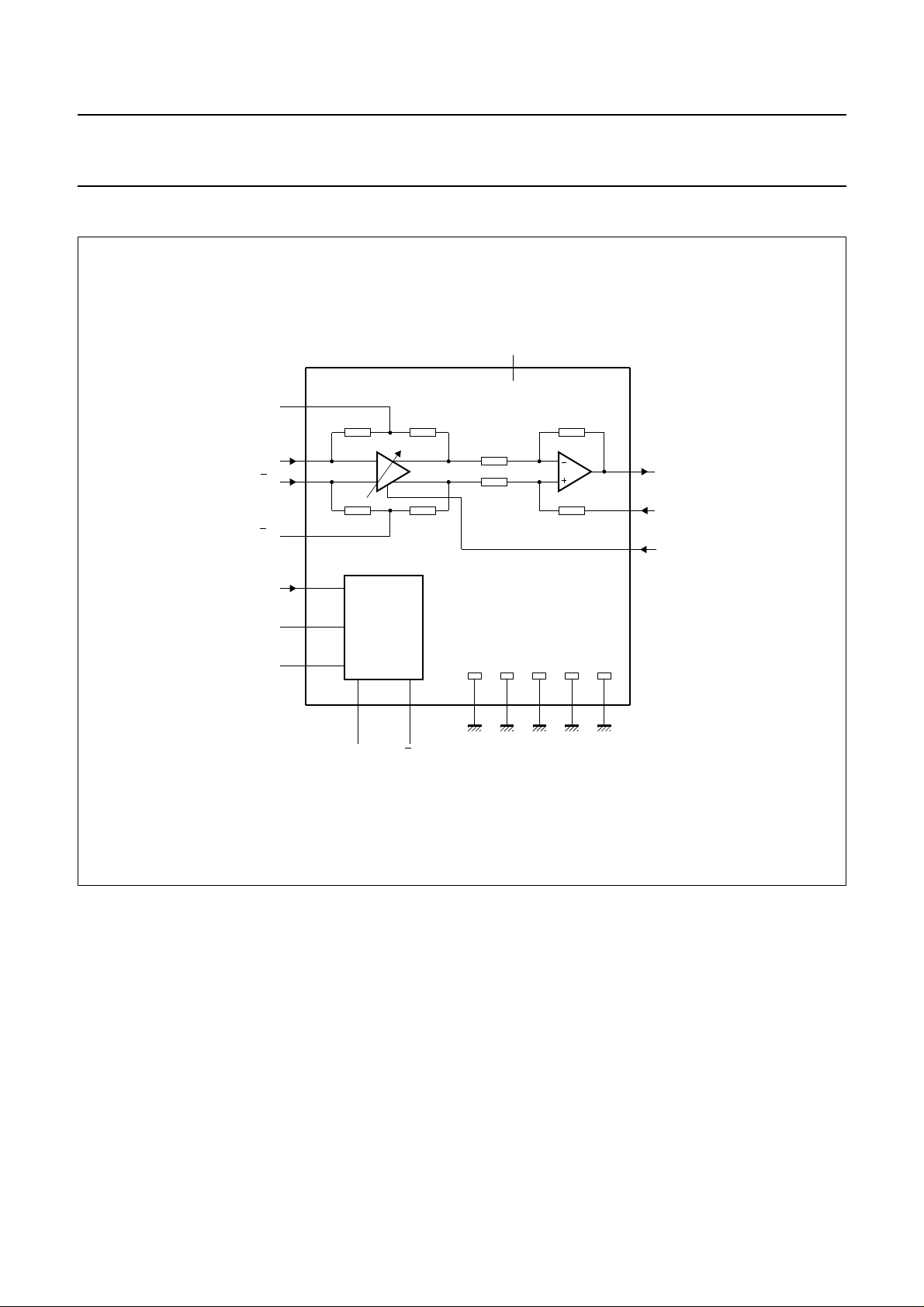
BLOCK DIAGRAM
book, full pagewidth
C
C
C
V
V
C
CE
DEC1
DEC2
V
P
11
6
lf
in
in
lf
100 k
1
20
100 k
15
16
3
CONTROL
18
R
100 k
Ω
Ω
100 k
Ω
20 k
Ω
20 k
Ω
Ω
20 k
20 k
Ω
13
8
Ω
17
TDA8780M
45 19
R
g
GND1 GND2 GND3 GND4 GND5
g
141072
V
out
V
ref
TEST
MBE161
Fig.1 Block diagram.
1995 Jul 25 3
Philips Semiconductors Product specification
True logarithmic amplifier TDA8780M
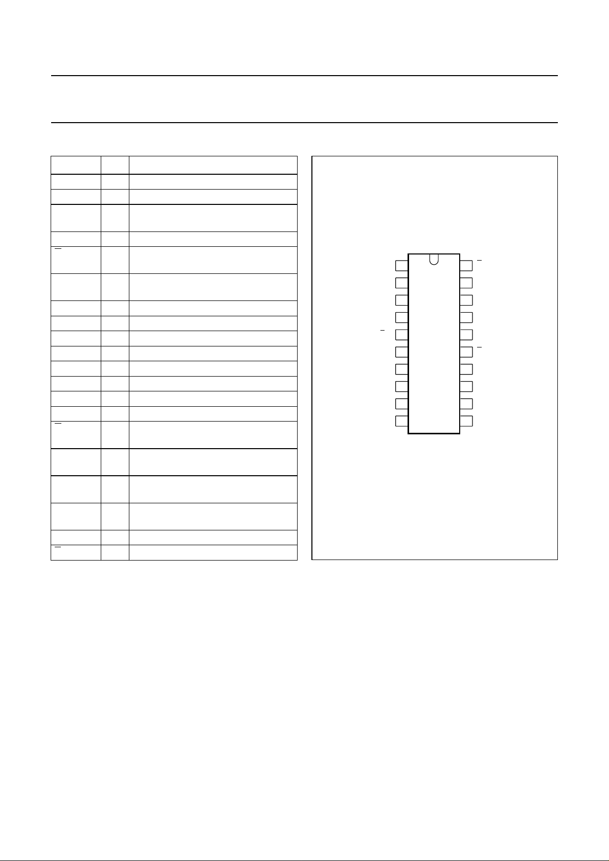
PINNING
SYMBOL PIN DESCRIPTION
V
in
GND1 2 ground 1
C
DEC1
R
g
R
g
C
lf
GND2 7 ground 2
V
ref
n.c. 9 not connected
GND3 10 ground 3 (main ground)
V
P
n.c. 12 not connected
V
out
GND4 14 ground 4
C
lf
CE 16 TTL-level-compatible circuit enable
TEST 17 test input; connected to ground in
C
DEC2
GND5 19 ground 5
V
in
1 signal voltage input
3 control circuit first decoupling and
optional start-up capacitor connection
4 small-signal gain-setting resistor
5 small-signal complementary
gain-setting resistor
6 low-frequency cut-off point setting
capacitor
8 external reference voltage input
11 power supply
13 true logarithmic voltage output
15 complementary low-frequency cut-off
point setting capacitor
input (active HIGH)
normal operation
18 control circuit second decoupling and
optional start-up capacitor
20 complementary signal voltage input
handbook, halfpage
V
1
in
GND1
2
C
3
DEC1
R
4
g
R
5
g
C
GND2
V
ref
n.c. n.c.
GND3
TDA8780M
6
lf
7
8
9
10
MBE160
Fig.2 Pin configuration.
V
20
in
GND5
19
C
18
DEC2
17
TEST
CE
16
C
15
lf
14
GND4
V
13
out
12
V
P
11
1995 Jul 25 4

Philips Semiconductors Product specification
True logarithmic amplifier TDA8780M
FUNCTIONAL DESCRIPTION
A true logarithmic amplifier can be realized from a cascade
of similar stages each stage consisting of a pair of
amplifiers whose inputs and outputs are connected in
parallel. One of these amplifiers can be formed by an
undegenerated long-tailed pair which provides high gain
but limited linear input signal-handling capability. The
other amplifier can be formed by a degenerated long-tailed
pair which provides a gain of unity and a much larger linear
input signal-handling capability.
The overall cascade amplifies very small input signals but,
once these reach the level at which the undegenerated
long-tailed pair in the last stage is at the limit of its linear
signal-handling capability, the output voltage becomes
logarithmically dependent on the input signal level. This
behaviour continues until the input signal reaches the level
at which undegenerated long-tailed pair in the first stage is
at the limit of its linear input signal-handling capability. The
transfer characteristic beyond this point then depends on
the exact configuration of the degenerated long-tailed pair
in the first stage.
Five stages are used in the TDA8780M to provide a 72 dB
true logarithmic dynamic range. The DC bias current in the
undegenerated long-tailed pair in the first stage is made
externally adjustable, using an off-chip resistor, to provide
a small-signal gain adjustment facility. The small signal
gain defined by this resistor is valid when the IC is
operating in the “linear” mode, for input signals typically
less than 60 µV.
A high-level limiter is inserted between the first and second
stages to provide a constant limiting output voltage which
is essentially independent of the value of the gain setting
resistor. These stages can be driven by single-ended or
differential inputs. The DC operating point is set by overall
on-chip feedback decoupled by two off-chip capacitors
which define the low-frequency cut-off point. The
performance is stabilized against temperature and DC
power supply variations. The input to the true logarithmic
amplifier is protected against damage due to excessive
differential input signals by diodes.
The differential output from the true logarithmic amplifier is
converted internally to a single-ended output by an on-chip
operational amplifier arrangement in which the DC output
level is set by an externally-supplied reference voltage.
The output is capable of driving loads down to 10 kΩ. The
limiting output voltage and the output drive capability have
been chosen to facilitate interfacing to analog-to-digital
converters. A major part of the DC power supply current
consumption of the device is associated with provision of
this output drive capability. The DC power supply
consumption is significantly less when the device is driving
smaller loads.
A power-down facility allows the circuit to be disabled from
a TTL-level compatible control input.
1995 Jul 25 5
 Loading...