

Philips TDA8779 Service Manual
INTEGRATED CIRCUITS
DATA SH EET
TDA8779
10-bit converter interface
(ADC/DAC) for quadrature
transceiver
Objective specification
Supersedes data of 1996 Sep 05
File under Integrated Circuits, IC02
1996 Sep 18
Philips Semiconductors Objective specification
10-bit converter interface (ADC/DAC) for
TDA8779
quadrature transceiver
FEATURES
• Two 10-bit ADCs with multiplexed outputs
• Two 10-bit DACs with multiplexed inputs
• Sampling rate for the ADCs and DACs up to 20 MHz
• Digital outputs (for the ADC) and inputs (for the DAC)
are TTL/CMOS compatible (2.7 to 5.5 V)
• Internal reference voltage regulator
• Power dissipation 520 mW
• Standby mode.
APPLICATIONS
Wireless communication.
QUICK REFERENCE DATA
SYMBOL PARAMETER CONDITIONS MIN. TYP. MAX. UNIT
V
CCA1
analog supply voltage for the
ADC part
V
CCD1
digital supply voltage for the
ADC part
V
CCA2
analog supply voltage for the
DAC part
V
CCD2
digital supply voltage for the
DAC part
V
CCO
I
CCA
I
CCD
I
CCO
f
CLK(ADC)max
output stage supply voltage 2.7 3.0 5.5 V
analog supply current − 71 − mA
digital supply current − 31 − mA
output stage supply current ramp input; f
maximum clock frequency for
the ADC part
INLA integral non linearity for the
ADC part
DNLA differential non linearity for
the ADC part
f
CLK(DAC)max
maximum clock frequency for
full-scale; ramp input;
f
=20MHz
CLK
50% full-scale; ramp input;
=20MHz
f
CLK
the DAC part
INLD integral non linearity for the
DAC part
DNLD differential non linearity for
the DAC part
P
tot
total power dissipation − 520 − mW
full-scale; ramp input;
=20MHz
f
CLK
full-scale; ramp input;
=20MHz
f
CLK
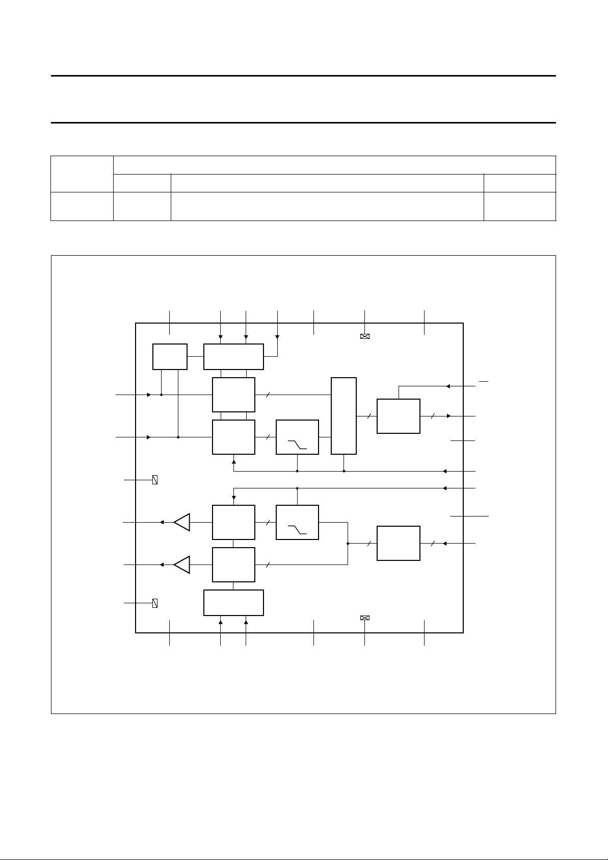
GENERAL DESCRIPTION
The TDA8779 contains two 10-bit high speed ADCs and
two 10-bit DACs for wireless communication (for use in
transceiver modules). This device converts two analog
input signals (channels I and Q) and digital inputs
(D0 to D9) at a maximum sampling rate of 20 MHz.
The input bias voltages for the analog input voltages are
provided internally at the middle code. The analog input
and output voltages are AC coupled.
The data sampling is performed on the rising edge of the
clock for ADCs and DACs.
All reference voltages are generated internally.
4.75 5.0 5.5 V
4.75 5.0 5.5 V
4.75 5.0 5.5 V
4.75 5.0 5.5 V
=20MHz − 2 − mA
CLK
20 −−MHz
−±2−LSB
−±0.3 − LSB
20 −−MHz
−±2−LSB
−±0.75 − LSB
1996 Sep 18 2
Philips Semiconductors Objective specification
10-bit converter interface (ADC/DAC) for
quadrature transceiver
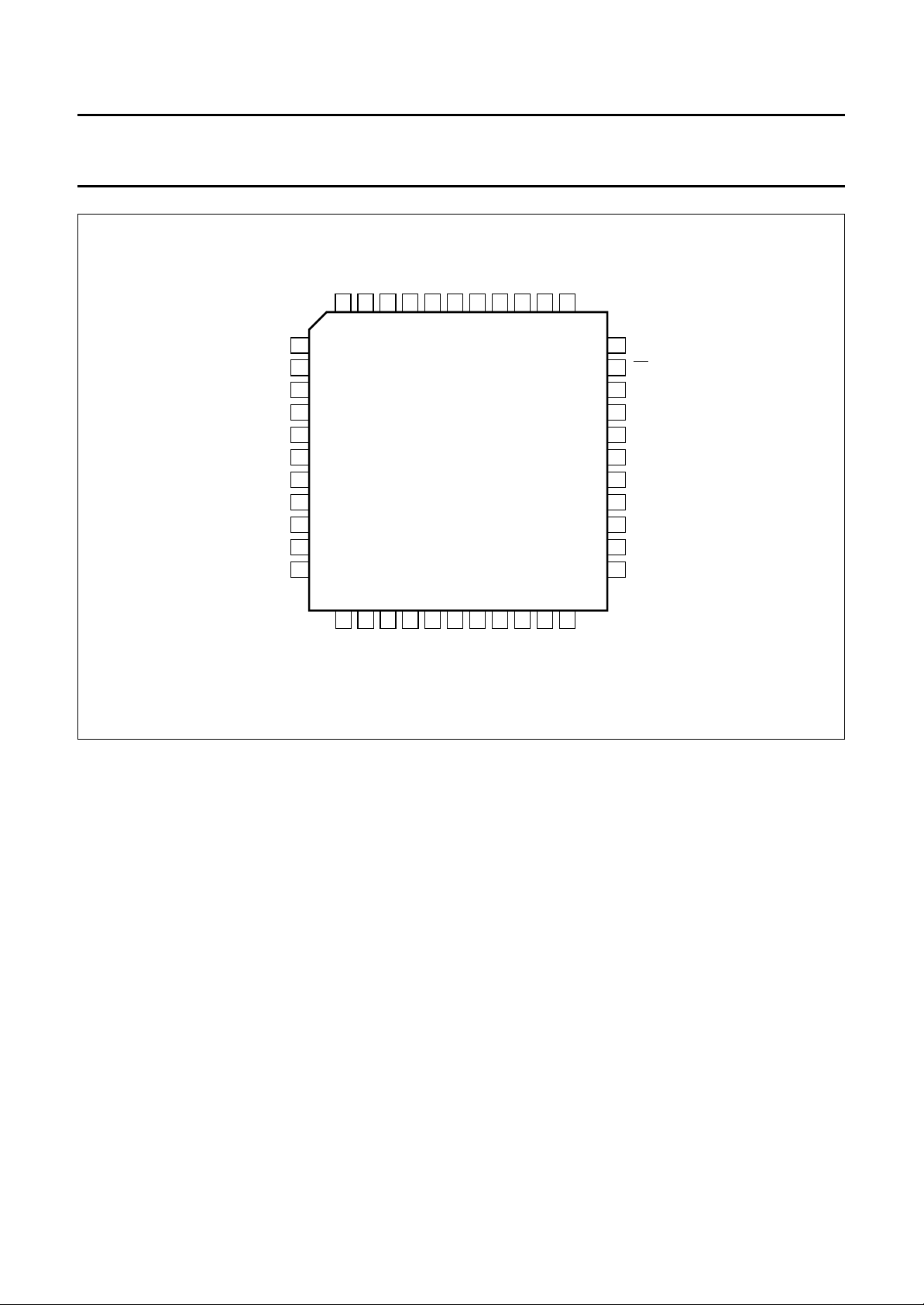
ORDERING INFORMATION
TYPE
NUMBER
TDA8779H QFP44
BLOCK DIAGRAM
handbook, full pagewidth
NAME DESCRIPTION VERSION
plastic quad flat package; 44 leads (lead length 1.3 mm);
body 10 × 10 × 1.75 mm
INI
INQ
4
6
V
CCA1
INPUT
BIAS
7
DEC2 DEC3
DEC1
23
REFERENCE
REGULATOR
10-BIT
ADC
10-BIT
ADC
10
10
5
LATCHES
PACKAGE
V
CCD1
31
DGND1
28
TDA8779
10 10
MUX
BUFFER
STDBYA
29
32
34-43
44
TDA8779
SOT307-2
OE
D0A to D9A
V
CCO
AGND1
OUTI
OUTQ
AGND2
30
1
BUFFER
9
BUFFER
11
13
8
V
CCA2
10-BIT
DAC
10-BIT
DAC
REFERENCE
REGULATOR
10
DEC5
DEC4
12
10
10
LATCHES
V
14
CCD2
10 10
BUFFER
25
DGND2
15-24
27
STDBYD
26
33
CLKA
CLKD
OGND
D0D to D9D
MGG075
Fig.1 Block diagram.
1996 Sep 18 3
Philips Semiconductors Objective specification
10-bit converter interface (ADC/DAC) for
quadrature transceiver
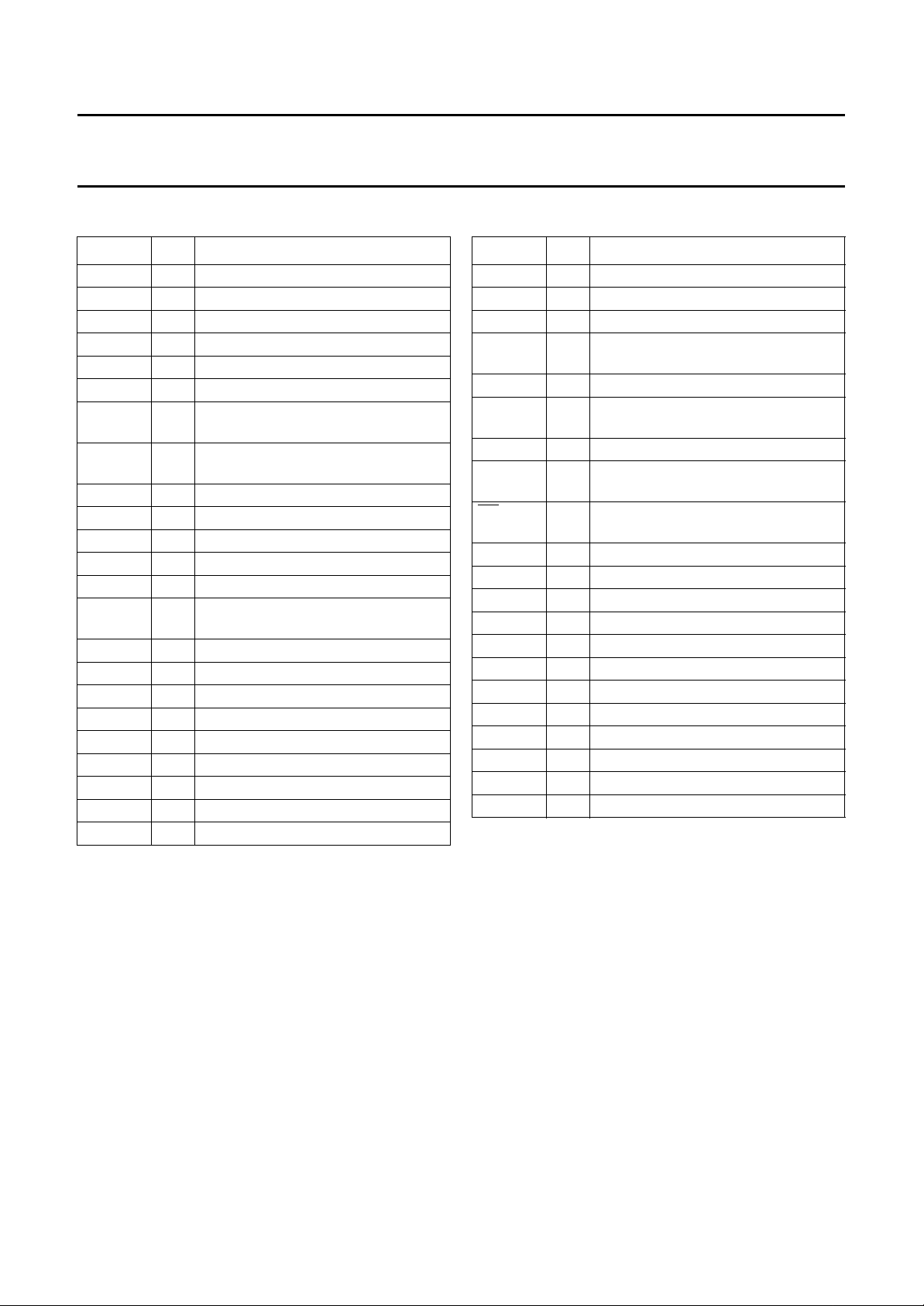
PINNING
SYMBOL PIN DESCRIPTION
AGND1 1 analog ground 1
DEC1 2 decoupling input 1
DEC2 3 decoupling input 2
INI 4 I channel ADC input
DEC3 5 decoupling input 3
INQ 6 Q channel ADC input
V
CCA1
V
CCA2
OUTI 9 I channel DAC analog output
DEC4 10 decoupling input 4
OUTQ 11 Q channel DAC analog output
DEC5 12 decoupling input 5
AGND2 13 analog ground 2
V
CCD2
D0D 15 multiplexed input for the DACs; bit 0
D1D 16 multiplexed input for the DACs; bit 1
D2D 17 multiplexed input for the DACs; bit 2
D3D 18 multiplexed input for the DACs; bit 3
D4D 19 multiplexed input for the DACs; bit 4
D5D 20 multiplexed input for the DACs; bit 5
D6D 21 multiplexed input for the DACs; bit 6
D7D 22 multiplexed input for the DACs; bit 7
D8D 23 multiplexed input for the DACs; bit 8
7 analog supply voltage 1 for ADC part
(+5 V)
8 analog supply voltage 2 for DAC part
(+5 V)
14 digital supply voltage 2 for DAC part
(+5 V)
TDA8779
SYMBOL PIN DESCRIPTION
D9D 24 multiplexed input for the DACs; bit 9
DGND2 25 digital ground 2
CLKD 26 transmission block clock
STDBYD 27 power standby for the DAC part
(active HIGH)
DGND1 28 digital ground 1
STDBYA 29 power standby for the ADC part
(active HIGH)
CLKA 30 reception block clock
V
CCD1
OE 32 ADCs digital output enable
OGND 33 input/output ground
D0A 34 I and Q digital outputs; bit 0
D1A 35 I and Q digital outputs; bit 1
D2A 36 I and Q digital outputs; bit 2
D3A 37 I and Q digital outputs; bit 3
D4A 38 I and Q digital outputs; bit 4
D5A 39 I and Q digital outputs; bit 5
D6A 40 I and Q digital outputs; bit 6
D7A 41 I and Q digital outputs; bit 7
D8A 42 I and Q digital outputs; bit 8
D9A 43 I and Q digital outputs; bit 9
V
CCO
31 digital supply voltage 1 for ADC part
(+5 V)
(3-state output); (active LOW)
44 output supply voltage (2.7 to 5.5 V)
1996 Sep 18 4
Philips Semiconductors Objective specification
10-bit converter interface (ADC/DAC) for
quadrature transceiver
handbook, full pagewidth
AGND1
DEC1
DEC2
INI
DEC3
INQ
V
CCA1
V
CCA2
OUTI
DEC4
OUTQ
1
2
3
4
5
6
7
8
9
10
11
CCO
V
44
D9A
43
D8A
42
D7A
D6A
41
40
TDA8779H
D5A
39
D4A
38
D3A
37
D2A
36
D1A
35
D0A
34
33
32
31
30
29
28
27
26
25
24
23
OGND
OE
V
CCD1
CLKA
STDBYA
DGND1
STDBYD
CLKD
DGND2
D9D
D8D
TDA8779
12
13
14
15
16
D0D
CCD2
D1D
DEC5
V
AGND2
Fig.2 Pin configuration.
17
D2D
18
D3D
19
D4D
20
D5D
21
D6D
22
D7D
MGG074
1996 Sep 18 5
Philips Semiconductors Objective specification
10-bit converter interface (ADC/DAC) for
TDA8779
quadrature transceiver
LIMITING VALUES
In accordance with the Absolute Maximum Rating System (IEC 134).
SYMBOL PARAMETER CONDITIONS MIN. MAX. UNIT
V
CCA1
V
CCA2
V
CCD1
V
CCD2
V
CCO
∆V
I
o
V
i
V
clk(p-p)
T
stg
T
amb
T
j
CC
analog supply voltage for ADC part −0.3 +7.0 V
analog supply voltage for DAC part −0.3 +7.0 V
digital supply voltage for ADC part −0.3 +7.0 V
digital supply voltage for DAC part −0.3 +7.0 V
output stage supply voltage −0.3 +7.0 V
voltage difference between:
V
V
V
CCA
CCA
CCD
− V
− V
− V
CCD
CCO
CCO
−1.0 +1.0 V
−1.0 +4.0 V
−1.0 +4.0 V
output current − 10 mA
input voltage referenced to AGND −0.3 +7.0 V
AC input switching voltage (peak-to-peak value) referenced to DGND − V
CCD
storage temperature −55 +150 °C
operating ambient temperature −20 +75 °C
junction temperature − 150 °C
V
THERMAL CHARACTERISTICS
SYMBOL PARAMETER CONDITIONS VALUE UNIT
R
th j-a
thermal resistance from junction to ambient in free air 75 K/W
CHARACTERISTICS
V
CCA=V7
V
CCO=V44
T
amb
and V8 to V1and V13= 4.75 to 5.5 V; V
CCD=V31
and V14 to V28and V25= 4.75 to 5.5 V;
to V33= 2.7 to 5.5 ; AGND1, AGND2, OGND, DGND1 and DGND2 are shorted together;
= −20 to +70 °C; measured typically at V
CCA=VCCD
= 5 V and V
=3V; CL= 15 pF; T
CCO
=25°C; unless
amb
otherwise specified.
SYMBOL PARAMETER CONDITIONS MIN. TYP. MAX. UNIT
Supplies
V
V
V
V
V
∆V
I
CCA
I
CCD
CCA1
CCD1
CCA2
CCD2
CCO
CC
analog supply voltage for ADC part 4.75 5.0 5.5 V
digital supply voltage for ADC part 4.75 5.0 5.5 V
analog supply voltage for DAC part 4.75 5.0 5.5 V
digital supply voltage for DAC part 4.75 5.0 5.5 V
output stage supply voltage 2.7 3.0 5.5 V
voltage difference between
V
V
V
CCA
CCA
CCD
− V
− V
− V
CCD
CCO
CCO
−0.2 − +0.2 V
−0.2 − +2.5 V
−0.2 − +2.5 V
analog supply current − 71 − mA
digital supply current − 31 − mA
1996 Sep 18 6
 Loading...