


TDA8777
Triple 10-bit video DAC, up to 330 MHz sample frequency
Rev. 03 — 15 August 2005 Preliminary data sheet
1. General description
The TDA8777consistsofthreeseparate10-bitvideoDigital-to-AnalogConverters (DACs)
with complementary outputs. They convert the digital input signals into analog current
outputs at a maximum conversion rate of 330 MHz.
The DACs are based on current source architecture.
A sync pulse can be added to the green signal (sync-on-green) to allow devices driven by
the video DAC to be synchronized.
The TDA8777 has a Power-down mode to reduce power consumption during inactive
periods.
The TDA8777 is fabricated in a CMOS process that ensures high functionality with low
power dissipation.
2. Features
■ Triple 10-bit DAC
■ Sampling frequency up to 330 MHz
■ Internal voltage reference (1.21 V)
■ Complementary outputs
■ Direct drive of double terminated 75 Ω load into standard level
■ TTL compatible input
■ Sync and blank control inputs
■ Analog output current source
■ Power-down mode
■ 3.3 V power supply
■ LQFP48 package
3. Applications
■ PC video cards
■ High resolution image processing
■ Digital video systems
■ General purpose high-speed digital-to-analog conversion

Philips Semiconductors
4. Quick reference data
Table 1: Quick reference data
Symbol Parameter Conditions Min Typ Max Unit
V
DDA
I
DDA
INL integral non-linearity −2 - +2 LSB
DNL differential non-linearity −1 - +1 LSB
f
CLK
P
tot
I
pd
5. Ordering information
TDA8777
Triple 10-bit video DAC, up to 330 MHz sample frequency
analog supply voltage 3.0 3.3 3.6 V
analog supply current - 90 - mA
clock frequency
TDA8777HL/14/C1 - - 140 MHz
TDA8777HL/24/C1 - - 240 MHz
TDA8777HL/33/C1 - - 330 MHz
total power dissipation - 297 - mW
current in Power-down mode - 20 - mA
Table 2: Ordering information
Type number Package Sampling
Name Description Version
TDA8777HL/14/C1 LQFP48 plastic low profile quad flat package;
TDA8777HL/24/C1 240 MHz
TDA8777HL/33/C1 330 MHz
48 leads; body 7 × 7 × 1.4 mm
SOT313-2 140 MHz
frequency
TDA8777_3 © Koninklijke Philips Electronics N.V. 2005. All rights reserved.
Preliminary data sheet Rev. 03 — 15 August 2005 2 of 18
Philips Semiconductors
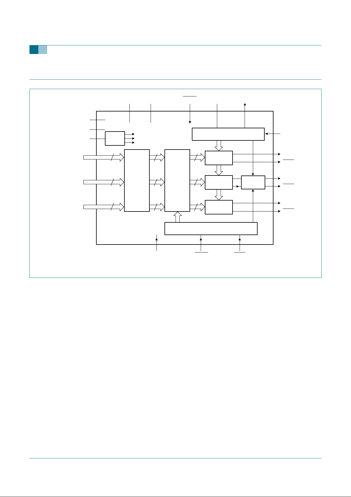
6. Block diagram
TDA8777
Triple 10-bit video DAC, up to 330 MHz sample frequency
V
DDA3
V
DDA2
V
DDA1
red digital
inputs
(bits R9 to R0)
green digital
inputs
(bits G9 to G0)
blue digital
inputs
(bits B9 to B0)
48-39
10-1
23-14
30
29
13
10
10
10
POR
V
SSA2
TRIPLE
MULTI-
PLEXER
V
SSA1
26
25
PSAVE
38
TDA8777
10
10
BLANKING
INSERT
10
24 12
10
10
10
DAC CONTROL MODULE
RSET
CURRENT/VOLTAGE REFERENCE
V
+ I
ref
ref
10-BIT DAC
V
+ I
ref
ref
10-BIT DAC
V
+ I
ref
ref
10-BIT DAC
11
BLANKCLK
COMP
SYNC
3537
I
ref
SYNC
INSERT
sync
36
VREF
34
OUTR
33
OUTR
32
OUTG
31
OUTG
28
OUTB
27
OUTB
mle290
Fig 1. Block diagram
TDA8777_3 © Koninklijke Philips Electronics N.V. 2005. All rights reserved.
Preliminary data sheet Rev. 03 — 15 August 2005 3 of 18
Philips Semiconductors
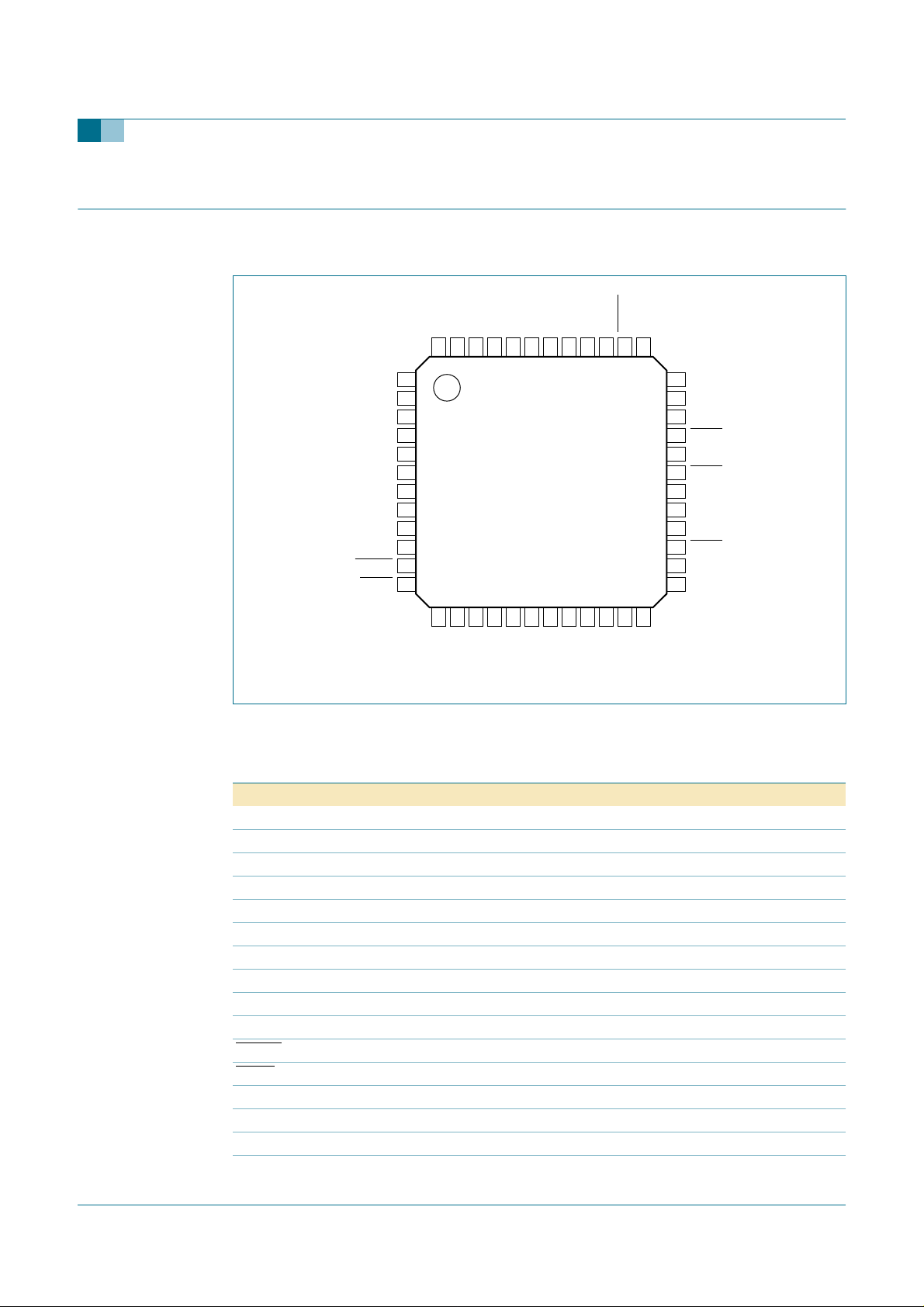
7. Pinning information
7.1 Pinning
TDA8777
Triple 10-bit video DAC, up to 330 MHz sample frequency
R9
4847464544434241403938
1
G0 VREF
2
G1 COMP
3
G2 OUTR
4
G3 OUTR
5
G4 OUTG
6
G5 OUTG
7
G6 V
8
G7 V
9
G8 OUTB
10
G9 OUTB
11
BLANK V
12
SYNC V
1314151617181920212223
DDA1
V
B0 R8
TDA8777HL
B1 R7
B2 R6
B3 R5
B4 R4
B5 R3
B6 R2
B7 R1
B8 R0
PSAVE
RSET
37
24
B9
CLK
36
35
34
33
32
31
30
DDA3
29
DDA2
28
27
26
SSA2
25
SSA1
001aad432
Fig 2. Pin configuration
7.2 Pin description
Table 3: Pin description
Symbol Pin Description
G0 1 green digital input data; bit 0 (LSB)
G1 2 green digital input data; bit 1
G2 3 green digital input data; bit 2
G3 4 green digital input data; bit 3
G4 5 green digital input data; bit 4
G5 6 green digital input data; bit 5
G6 7 green digital input data; bit 6
G7 8 green digital input data; bit 7
G8 9 green digital input data; bit 8
G9 10 green digital input data; bit 9 (MSB)
BLANK 11 composite blank control input (active LOW)
SYNC 12 composite sync control input; for green channel only (active LOW)
V
DDA1
B0 14 blue digital input data; bit 0 (LSB)
B1 15 blue digital input data; bit 1
B2 16 blue digital input data; bit 2
13 analog supply voltage 1
TDA8777_3 © Koninklijke Philips Electronics N.V. 2005. All rights reserved.
Preliminary data sheet Rev. 03 — 15 August 2005 4 of 18

Philips Semiconductors
TDA8777
Triple 10-bit video DAC, up to 330 MHz sample frequency
Table 3: Pin description
Symbol Pin Description
B3 17 blue digital input data; bit 3
B4 18 blue digital input data; bit 4
B5 19 blue digital input data; bit 5
B6 20 blue digital input data; bit 6
B7 21 blue digital input data; bit 7
B8 22 blue digital input data; bit 8
B9 23 blue digital input data; bit 9 (MSB)
CLK 24 clock input
V
SSA1
V
SSA2
OUTB 27 complementary blue current analog output
OUTB 28 blue current analog output
V
DDA2
V
DDA3
OUTG 31 complementary green current analog output
OUTG 32 green current analog output
OUTR 33 complementary red current analog output
OUTR 34 red current analog output
COMP 35 compliance voltage output
VREF 36 voltage reference input
RSET 37 full-scale current control resistor pin
PSAVE 38 power-save control input (active LOW)
R0 39 red digital input data; bit 0 (LSB)
R1 40 red digital input data; bit 1
R2 41 red digital input data; bit 2
R3 42 red digital input data; bit 3
R4 43 red digital input data; bit 4
R5 44 red digital input data; bit 5
R6 45 red digital input data; bit 6
R7 46 red digital input data; bit 7
R8 47 red digital input data; bit 8
R9 48 red digital input data; bit 9 (MSB)
25 analog supply ground 1
26 analog supply ground 2
29 analog supply voltage 2
30 analog supply voltage 3
…continued
8. Functional description
This triple 10-bit video DAC is designed to convert digital input signals into analog output
currents. All inputs (clock, data, blank and sync) must be TLL levels.
8.1 Voltage reference
The voltage referenceinputtopin VREF should be 1.21 V.For correct operation, a 100 nF
capacitor should be connected between pin VREF and pin V
TDA8777_3 © Koninklijke Philips Electronics N.V. 2005. All rights reserved.
Preliminary data sheet Rev. 03 — 15 August 2005 5 of 18
DDA
.
Philips Semiconductors
An external reference resistor must be connected between pin RSET and analog ground.
This resistor sets the reference current which determines the analog output level, and is
specified to be 560 Ω. This value allows a 1 V (p-p) output (video plus sync) into a 37.5 Ω
load, such as a double-terminated 75 Ω coaxial cable.
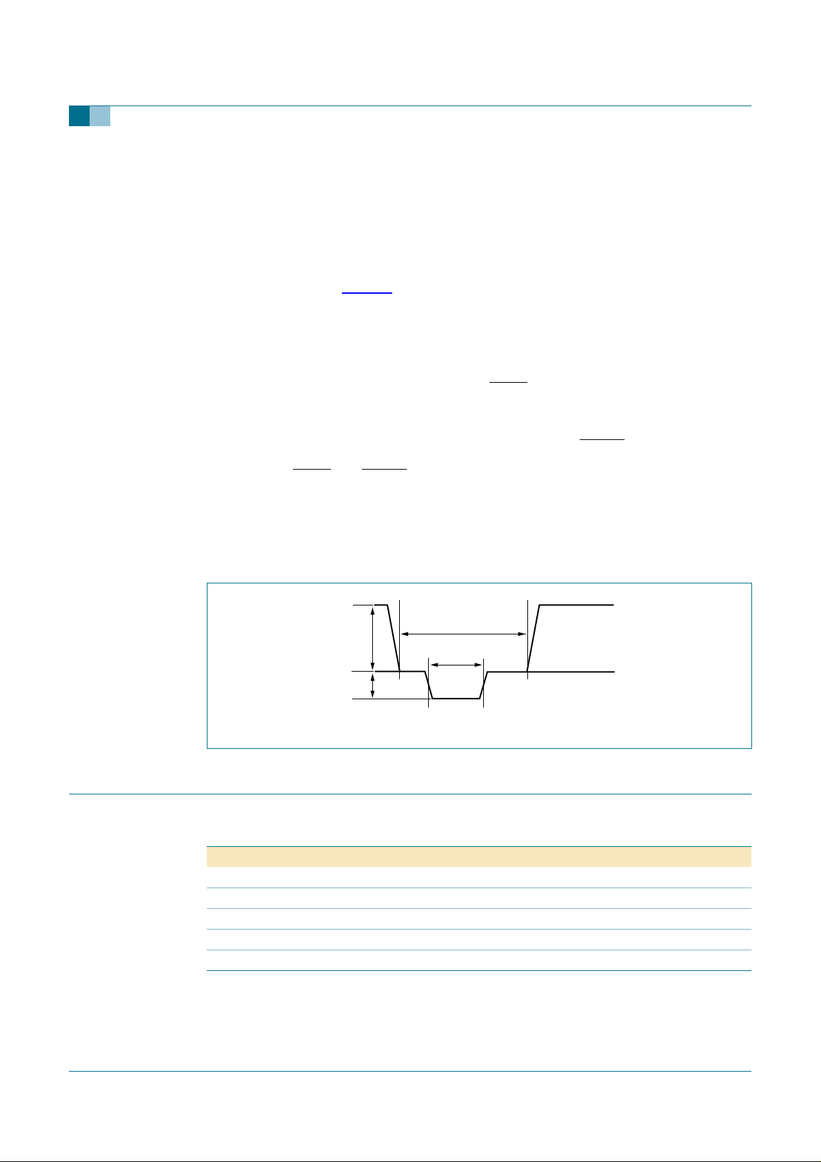
8.2 Blanking and sync pulse insertion
The video signal (see Figure 3) is comprised of the following three parts:
• The video information: defined by the 10 bits used to drive the DAC; nominal signal
amplitude = 700 mV (p-p)
• The sync pulse: a horizontal synchronization (hsync) pulse indicates the end of a
video line and the start of the next video line; sync nominal amplitude = 300 mV; sync
is added to the video signal output via the SYNC input (active LOW)
• The blanking period: allows interface-free detection of both sync and video, blanking
is allocated either side of the sync pulse; the blank level is equal to the video black
level; blanking is added to the video signal output via the BLANK input (active LOW).
The values of SYNC and BLANK are latched on the rising edge of the clock signal. When
no sync and no blank are applied, the DAC can be used continuously. This is the so-called
generic mode.
TDA8777
Triple 10-bit video DAC, up to 330 MHz sample frequency
Because the signal delay in the DACis 1.5 times the clock period, the sync and blank are
also delayed by 1.5 times the clock period.
Fig 3. Video signal sync pulse and blanking period
9. Limiting values
Table 4: Limiting values
In accordance with the Absolute Maximum Rating System (IEC 60134).
Symbol Parameter Conditions Min Max Unit
V
DDA
V
n
T
stg
T
amb
T
j
0.7 V
0.3 V
analog supply voltage referred to V
voltage on digital input pins referred to V
storage temperature −55 +150 °C
ambient temperature 0 70 °C
junction temperature −40 +125 °C
blanking period
sync pulse
video information
SSA1
SSA2
mle291
−0.5 +6.5 V
−0.5 +5.5 V
TDA8777_3 © Koninklijke Philips Electronics N.V. 2005. All rights reserved.
Preliminary data sheet Rev. 03 — 15 August 2005 6 of 18
 Loading...