

Philips tda8776 DATASHEETS
INTEGRATED CIRCUITS
DATA SH EET
TDA8776
10-bit, 500 Msps Digital-to-Analog
Converter (DAC)
Product specification
Supersedes data of 1995 Mar 28
File under Integrated Circuits, IC02
1996 Jun 04
Philips Semiconductors Product specification
10-bit, 500 Msps Digital-to-Analog
TDA8776
Converter (DAC)
FEATURES
• 10-bit resolution
• Conversion rate up to 500 MHz
• 10K/100K ECL input levels
• Internal reference voltage generator
• No deglitching circuit required
• Internal input register
• Power dissipation only 925 mW (typical)
• Internal 50 Ω output load (connected to the analog
ground)
• Very few external components required.
QUICK REFERENCE DATA
SYMBOL PARAMETER CONDITIONS MIN. TYP. MAX. UNIT
V
V
V
EEA
EED
EEI
analog supply voltage −5.46 −5.20 −4.94 V
digital supply voltage −5.46 −5.20 −4.94 V
input stages digital supply
note 1 −5.46 −5.20 −4.94 V
voltage
I
EEA
I
EED
I
EEI
analog supply current note 1 − 108 145 mA
digital supply current note 1 − 60 85 mA
input stages digital supply
note 1 − 10 15 mA
current
V
OUT
− V
OUT
full-scale analog output voltage
notes 1 and 2; ZL=50Ω 1.7 2.0 2.5 V
(peak-to-peak value)
INL DC integral non-linearity note 3 −±0.3 ±0.5 LSB
DNL DC differential non-linearity note 3 −±0.2 ±0.45 LSB
f
clk(max)
t
S1
P
tot
maximum clock frequency 500 −−MHz
settling time (differential) 10% to 90% full scale; Fig.9 − 0.5 − ns
total power dissipation − 925 − mW
APPLICATIONS
High-speed digital-to-analog conversion for:
• High resolution video and graphics
• Direct Digital Synthesis (DDS)
• Telecommunication
• High-speed modems.
GENERAL DESCRIPTION
The TDA8776 is a 10-bit Digital-to-Analog Converter
(DAC) for high resolution video and other high frequency
applications. It converts the digital input signal into an
analog output voltage at a maximum conversion rate of
500 Msps. No external reference voltage is required and
all digital inputs are 10K/100K-ECL compatible.
Notes
1. D0 to D9 connected to either HIGH or LOW level, CLK is HIGH and CLK is LOW.
2. The analog output voltages (V
resistance between AGND and each of these outputs is typically 50 Ω.
3. A warm-up time is necessary to reach optimal performances.
ORDERING INFORMATION
TYPE NUMBER
TDA8776K PLCC28 plastic leaded chip carrier; 28 leads SOT261-2
1996 Jun 04 2
OUT
and V
) are negative with respect to AGND (see Table 1). The external output
OUT
PACKAGE
NAME DESCRIPTION VERSION
Philips Semiconductors Product specification
10-bit, 500 Msps Digital-to-Analog
Converter (DAC)
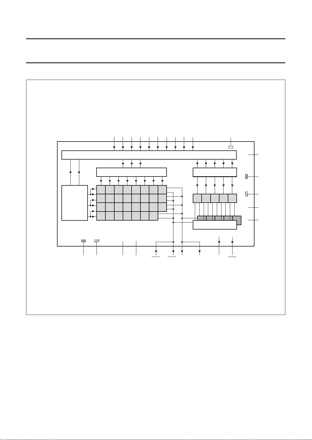
BLOCK DIAGRAM
handbook, full pagewidth
ROW
DECODER
D9 D8 D7 D6 D5 D4 D3 D2
22 21 20 19 18 17 16 15 14 13 12
COLUMN DECODER
TDA8776
ECL BUFFERS
D1 D0 IGND
DELAY
R-2R DIVIDER
TDA8776
25
V
EEI
28
DGND2
10
AGND2
11
V
EED3
24
V
EEA
25 34 9 86 7 27
DGND1
AGND1
V
EED1VEED2
V
OUT2
V
OUT1VOUT1VOUT2
Fig.1 Block diagram.
26
MLD200
CLK CLK
1996 Jun 04 3
Philips Semiconductors Product specification
10-bit, 500 Msps Digital-to-Analog
Converter (DAC)
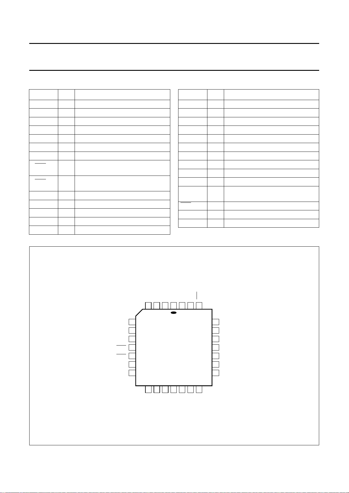
PINNING
SYMBOL PIN DESCRIPTION
n.c. 1 not connected
DGND1 2 digital ground 1
V
EED1
V
EED2
AGND1 5 analog ground 1
V
OUT1
V
OUT2
V
OUT1
V
OUT2
AGND2 10 analog ground 2
V
EED3
IGND 12 input ground for ECL input buffers
D0 13 data input; bit 0 (LSB)
D1 14 data input; bit 1
3 digital supply voltage 1 (−5.2 V)
4 digital supply voltage 2 (−5.2 V)
6 analog voltage output 1
7 analog voltage output 2
8 complementary analog voltage
output 1
9 complementary analog voltage
output 2
11 digital supply voltage 3 (−5.2 V)
TDA8776
SYMBOL PIN DESCRIPTION
D2 15 data input; bit 2
D3 16 data input; bit 3
D4 17 data input; bit 4
D5 18 data input; bit 5
D6 19 data input; bit 6
D7 20 data input; bit 7
D8 21 data input; bit 8
D9 22 data input; bit 9 (MSB)
n.c. 23 not connected
V
EEA
V
EEI
CLK 26 complementary clock input
CLK 27 clock input
DGND2 28 digital ground 2
24 analog supply voltage (−5.2 V)
25 input supply voltage for ECL input
buffers (−5.2 V)
handbook, halfpage
EED2VEED1
AGND1
V
OUT1
V
OUT2
V
OUT1
V
OUT2
AGND2
V
EED3
V
5
6
7
8
9
10
11
4
12
IGND
DGND1
3
2
TDA8776
13
14
D0
D1D2D3
Fig.2 Pin configuration.
1996 Jun 04 4
n.c.
1
15
CLK
DGND2
28
27
16
17
D4
CLK
26
18
D5
25
24
23
22
21
20
19
MLD201
V
V
n.c.
D9
D8
D7
D6
EEI
EEA
Philips Semiconductors Product specification
10-bit, 500 Msps Digital-to-Analog
TDA8776
Converter (DAC)
LIMITING VALUES
In accordance with the Absolute Maximum Rating System (IEC 134).
SYMBOL PARAMETER CONDITIONS MIN. MAX. UNIT
V
EEA
V
EED
V
EEI
− V
V
EEA
EED
AGND − DGND ground voltage differential −0.1 +0.1 V
V
I
I
OUT/IOUT
T
stg
T
amb
T
j
HANDLING
Inputs and outputs are protected against electrostatic discharges in normal handling. However, to be totally safe, it is
desirable to take normal precautions appropriate to handling integrated circuits.
analog supply voltage −7.0 ±0.3 V
digital supply voltage −7.0 ±0.3 V
input stages digital supply voltage −7.0 ±0.3 V
supply voltage differential −0.5 +0.5 V
input voltage V
EEI
±0.3 V
total output current ZL=50Ω−5 +50 mA
storage temperature −55 +150 °C
operating ambient temperature 0 +70 °C
junction temperature − +150 °C
THERMAL CHARACTERISTICS
SYMBOL PARAMETER VALUE UNIT
R
th j-a
thermal resistance from junction to ambient in free air 55 (typ.) K/W
1996 Jun 04 5
Philips Semiconductors Product specification
10-bit, 500 Msps Digital-to-Analog
TDA8776
Converter (DAC)
CHARACTERISTICS
V
EEA=V24
V
EEI=V25
shorted together; V
V
EEA=VEED
Supply
V
EEA
V
EED
V
EEI
I
EEA
I
EED
I
EEI
AGND − DGND ground voltage differential −0.1 − +0.1 V
Inputs
DIGITAL INPUTS (D9 TO D0) AND CLOCK INPUTS (CLK AND CLK)
V
IL
V
IH
I
IL
I
IH
f
clk(max)
Outputs (referenced to AGND); notes 1 and 2
V
OUT
Z
O
Transfer function
INL DC integral non-linearity note 3 −±0.3 ±0.5 LSB
DNL DC differential non-linearity note 3 −±0.2 ±0.45 LSB
to V5and V10= −5.46 to −4.94 V; V
to V12= −5.46 to −4.94 V; V
− V
OUT
= −5.2 V and T
= 2 V (p-p); ZL=50Ω; unless otherwise specified (typical values measured at
OUT
=25°C).
amb
EED
and V
EED=V3,V4
shorted together; T
EEI
and V11to V2and V28= −5.46 to −4.94 V;
= 0 to +70 °C; AGND, DGND and IGND
amb
SYMBOL PARAMETER CONDITIONS MIN. TYP. MAX. UNIT
analog supply voltage −5.46 −5.20 −4.94 V
digital supply voltage −5.46 −5.20 −4.94 V
input stages digital supply voltage note 1 −5.46 −5.20 −4.94 V
analog supply current note 1 − 108 145 mA
digital supply current note 1 − 60 85 mA
input stages digital supply current note 1 − 10 15 mA
LOW level input voltage −1.9 −1.8 −1.6 V
HIGH level input voltage −1.2 −0.9 −0.8 V
LOW level input current VI= −1.8 V −−10 µA
HIGH level input current VI= −0.9 V −−20 µA
maximum clock frequency 500 −−MHz
− V
OUT
full-scale analog output voltage
ZL=50Ω 1.7 2.0 2.5 V
(peak-to-peak value)
output impedance − 50 −Ω
Spurious free dynamic range (f
SFDR spurious free dynamic range
1996 Jun 04 6
= 500 MHz); V
clk
= 10 MHz −65 −69 − dB
f
OUT
= 50 MHz −−60 − dB
f
OUT
= 80 MHz −−59 − dB
f
OUT
= 100 MHz −52 −59 − dB
f
OUT
EEA=VEED
= 5.2 V; T
=25°C; note 4; see Fig.3
amb
 Loading...