

Philips TDA8771H-C2-R1, TDA8775G-C1 Datasheet
DATA SH EET
Preliminary specification
File under Integrated Circuits, IC02
1996 Aug 14
INTEGRATED CIRCUITS
TDA8775
Triple 10-bit video Digital-to-Analog
Converter (DAC)
1996 Aug 14 2
Philips Semiconductors Preliminary specification
Triple 10-bit video Digital-to-Analog
Converter (DAC)
TDA8775
FEATURES
• 10-bit resolution
• Sampling rate up to:
– 50 MHz for normal mode; RL= 37.5 Ω
– 35 MHz for LOW power mode; RL= 150 Ω
• Internal current reference
• Current reference selector for:
– normal mode, RL= 37.5 Ω (typ.)
– low-power mode, RL= 150 Ω (typ.)
• No deglitching circuit required
•
SYNC and BLANK control inputs
• 0.66 V output voltage range on red and blue channels
• 1 V output voltage range on green channel
(including sync)
• BLANK control input on the 3 channels
• + 5 V power supply.
APPLICATIONS
• General purpose high-speed digital-to-analog
conversion
• Digital TV
• Graphic display
• Desktop video processing.
GENERAL DESCRIPTION
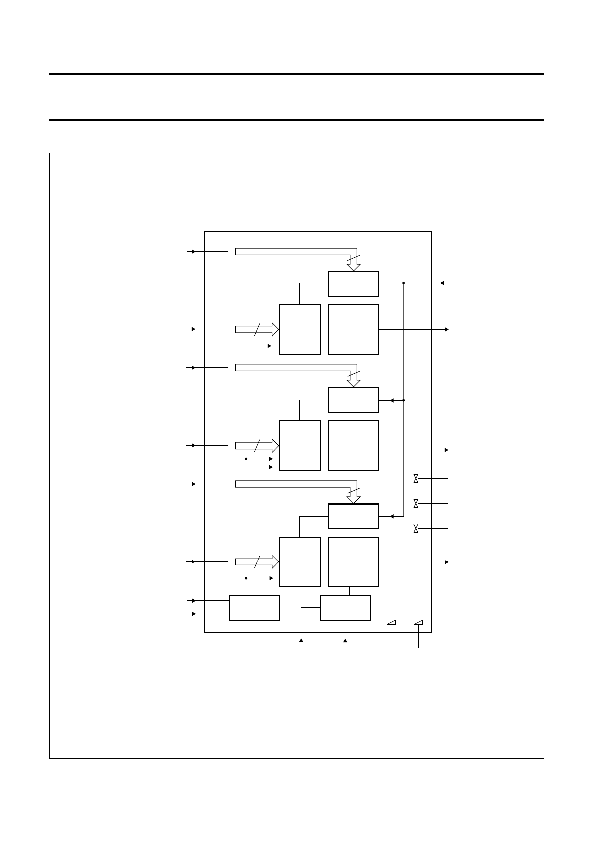
The TDA8775 consists of three 10-bit video
Digital-to-Analog Converters (DACs). They convert the
digital input signals into current outputs at a maximum
conversion rate of 50 MHz.
The DACs are based on current source architecture with
selectable current reference.
The devices are fabricated in a 5 V CMOS process that
ensures high functionality with low power dissipation.
QUICK REFERENCE DATA
ORDERING INFORMATION
SYMBOL PARAMETER CONDITIONS MIN. TYP. MAX. UNIT
V
DDA
analog supply voltage 4.5 5.0 5.5 V
V
DDD
digital supply voltage 4.5 5.0 5.5 V
I
DDA
analog supply current SLT = 1; RL= 37.5 Ω−67 tbf mA
SLT = 0; R
L
= 150 Ω−16 tbf mA
I
DDD
digital supply current SLT = 1; RL= 37.5 Ω−15 tbf mA
SLT = 0; R
L
= 150 Ω−10 tbf mA
INL DC integral non-linearity −±1±2 LSB
DNL DC differential non-linearity −±0.7 ±1.0 LSB
f
clk(max)
maximum clock frequency SLT = 1; RL= 37.5 Ω 50 −−MHz
SLT = 0; R
L
= 150 Ω 35 −−MHz
P
tot
total power dissipation SLT = 1; RL= 37.5 Ω;
f
clk
=50MHz
− 410 tbf mW
SLT = 0; R
L
= 150 Ω;
f
clk
=35MHz
− 130 tbf mW
TYPE
NUMBER
PACKAGE
NAME DESCRIPTION VERSION
TDA8775G LQFP48 plastic low profile quad flat package; 48 leads; body 7 × 7 × 1.4 mm SOT313-2
1996 Aug 14 3
Philips Semiconductors Preliminary specification
Triple 10-bit video Digital-to-Analog
Converter (DAC)
TDA8775
BLOCK DIAGRAM
Fig.1 Block diagram.
handbook, full pagewidth
MGE965
6
6
10-7
6-1
24-21
20-15
35-32
31-26
14
13
48 39 12 36
42
40
43
47
44
46
25
11454138
6
4
4
4
CURRENT
SOURCE
MSB
DECODER
LSB
DECODER
CURRENT
REFERENCE
CURRENT
SOURCE
MSB
DECODER
LSB
DECODER
CURRENT
SOURCE
MSB
DECODER
LSB
DECODER
CONTROL
REGISTER
V
DDA1VDDA2VDDA3
V
DDD1
37
V
DDD2
OUTB
OUTG
OUTR
VSSA1
VSSA2
VSSA3
CLK
SLT reference current
decoupling input
(I
ref
)
V
SSD1VSSD2
red
digital inputs
(bits R0 to R3)
red
digital inputs
(bits R4 to R9)
green
digital inputs
(bits G0 to G3)
green
digital inputs
(bits G4 to G9)
blue
digital inputs
(bits B0 to B3)
blue
digital inputs
(bits B4 to B9)
BLANK
control input
SYNC
control input
TDA8775
1996 Aug 14 4
Philips Semiconductors Preliminary specification
Triple 10-bit video Digital-to-Analog
Converter (DAC)
TDA8775
PINNING
SYMBOL PIN DESCRIPTION
R9 1 red digital input data; bit 9 (MSB)
R8 2 red digital input data; bit 8
R7 3 red digital input data; bit 7
R6 4 red digital input data; bit 6
R5 5 red digital input data; bit 5
R4 6 red digital input data; bit 4
R3 7 red digital input data; bit 3
R2 8 red digital input data; bit 2
R1 9 red digital input data; bit 1
R0 10 red digital input data; bit 0 (LSB)
V
DDD1
11 digital supply voltage 1
V
SSD1
12 digital supply ground 1
SYNC 13 composite sync control input; for green channel only (active LOW)
BLANK 14 composite blank control input (active LOW)
G9 15 green digital input data; bit 9 (MSB)
G8 16 green digital input data; bit 8
G7 17 green digital input data; bit 7
G6 18 green digital input data; bit 6
G5 19 green digital input data; bit 5
G4 20 green digital input data; bit 4
G3 21 green digital input data; bit 3
G2 22 green digital input data; bit 2
G1 23 green digital input data; bit 1
G0 24 green digital input data; bit 0 (LSB)
CLK 25 clock input
B9 26 blue digital input data; bit 9 (MSB)
B8 27 blue digital input data; bit 8
B7 28 blue digital input data; bit 7
B6 29 blue digital input data; bit 6
B5 30 blue digital input data; bit 5
B4 31 blue digital input data; bit 4
B3 32 blue digital input data; bit 3
B2 33 blue digital input data; bit 2
B1 34 blue digital input data; bit 1
B0 35 blue digital input data; bit 0 (LSB)
V
SSD2
36 digital supply ground 2
V
DDD2
37 digital supply voltage 2
V
DDA1
38 analog supply voltage 1
I
ref
39 decoupling pin for reference current
V
SSA1
40 analog supply ground 1
1996 Aug 14 5
Philips Semiconductors Preliminary specification
Triple 10-bit video Digital-to-Analog
Converter (DAC)
TDA8775
V
DDA2
41 analog supply voltage 2
OUTB 42 blue analog output
V
SSA2
43 analog supply ground 2
OUTG 44 green analog output
V
DDA3
45 analog supply voltage 3
OUTR 46 red analog output
V
SSA3
47 analog supply ground 3
SLT 48 mode selection; normal mode, R
L
= 37.5 Ω (active HIGH); low power mode,
RL= 150 Ω (active LOW)
SYMBOL PIN DESCRIPTION
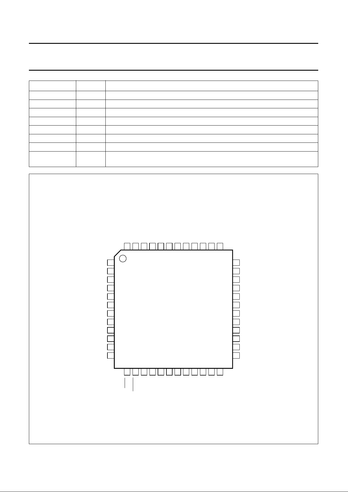
Fig.2 Pin configuration.
handbook, full pagewidth
1
2
3
4
5
6
7
8
9
10
11
36
35
34
33
32
31
30
29
28
27
26
13
14
15
16
17
18
19
20
21
22
23
48
47
46
45
44
43
42
41
40
39
38
12
24 37
25
TDA8775
MGE964
V
SSD2
B0
B1
B2
B4
B5
B6
B7
B8
B9
CLK
R9
R8
R7
R6
R5
R4
R2
R1
V
DDD1
V
SSD1
B3
V
SSA3
OUTR
V
DDA3
OUTG
V
SSA2
OUTB
V
SSA1
I
ref
V
DDA1
V
DDD2
SLT
V
DDA2
R3
R0
G9
G8
G7
G6
G5
G4
G2
G1
G0
G3
BLANK
SYNC
 Loading...