

Philips TDA8772AH-3, TDA8772H-8, TDA8772H-3, TDA8772AH-8 Datasheet
DATA SH EET
Product specification
Supersedes data of May 1994
File under Integrated Circuits, IC02
1995 Mar 09
INTEGRATED CIRCUITS
Philips Semiconductors
TDA8772; TDA8772A
Triple 8-bit video digital-to-analog
converter
1995 Mar 09 2
Philips Semiconductors Product specification
Triple 8-bit video digital-to-analog
converter
TDA8772; TDA8772A
FEATURES
• 8-bit resolution
• Sampling rate up to
35 MHz for TDA8772H/3, TDA8772AH/3
85 MHz for TDA8772H/8, TDA8772AH/8
• Internal reference voltage regulator
• No deglitching circuit required
• SYNC, BLANK control inputs
• 3 independent clock inputs (one per DAC)
• 1 V output voltage range
• 75 Ω output load
• TDA8772A has
BLANK control input on the GREEN
channel only while TDA8772 has it on the 3 channels
• Single 5 V power supply
• 44-pin QFP package.
APPLICATIONS
• General purpose high-speed digital-to-analog
conversion
• Digital TV
• Graphic display
• Desktop video processing.
GENERAL DESCRIPTION
The TDA8772, TDA8772A are triple 8-bit video
digital-to-analog converters (DACs). They convert the
digital input signals into analog voltage outputs at a
maximum conversion rate of 35 MHz (TDA8772H/3,
TDA8772AH/3) and 85 MHz (TDA8772H/8,
TDA8772AH/8).
The DACs are based on resistor-string architecture with
integrated output buffers. The output voltage range is
determined by a built-in reference source.
The devices are fabricated in a 5 V CMOS process that
ensures high functionality with low power dissipation.
ORDERING INFORMATION
TYPE NUMBER
PACKAGE
SAMPLING
FREQUENCY
PINS PIN POSITION MATERIAL CODE
TDA8772H/3 44 QFP44 plastic SOT307B 35 MHz
TDA8772AH/3 44 QFP44 plastic SOT307B 35 MHz
TDA8772H/8 44 QFP44 plastic SOT307B 85 MHz
TDA8772AH/8 44 QFP44 plastic SOT307B 85 MHz
1995 Mar 09 3
Philips Semiconductors Product specification
Triple 8-bit video digital-to-analog
converter
TDA8772; TDA8772A
QUICK REFERENCE DATA
Note
1. Minimum and maximum data of current and power consumption are measured in worse case conditions: for
minimum data, all digital inputs are at logic level 0 while for maximum data, all digital inputs are at logic level 1.
SYMBOL PARAMETER CONDITIONS MIN. TYP. MAX. UNIT
V
DDA
analog supply voltage 4.5 5.0 5.5 V
V
DDD
digital supply voltage 4.5 5.0 5.5 V
I
DDA
analog supply current RL=75Ω; note 1 40 65 100 mA
I
DDD
digital supply current
TDA8772H/3, TDA8772AH/3 − 716mA
TDA8772H/8, TDA8772AH/8 − 16 27 mA
INL integral non-linearity2 f
clk
= 35 MHz; ramp input −±0.5 ±1 LSB
f
clk
= 85 MHz; ramp input −±0.75 ±1.2 LSB
DNL differential non-linearity f
clk
= 35 MHz; ramp input −±0.25 ±0.5 LSB
f
clk
= 85 MHz; ramp input - ±0.5 ±0.75 LSB
f
clk(max)
maximum clock frequency
TDA8772H/3, TDA8772AH/3 35 −−MHz
TDA8772H/8, TDA8772AH/8 85 −−MHz
P
tot
total power dissipation note 1
TDA8772H/3, TDA8772AH/3 R
L
=75Ω; f
clk
= 35 MHz 180 360 640 mW
TDA8772H/8, TDA8772AH/8 R
L
=75Ω; f
clk
= 85 MHz 180 405 700 mW
1995 Mar 09 4
Philips Semiconductors Product specification
Triple 8-bit video digital-to-analog
converter
TDA8772; TDA8772A
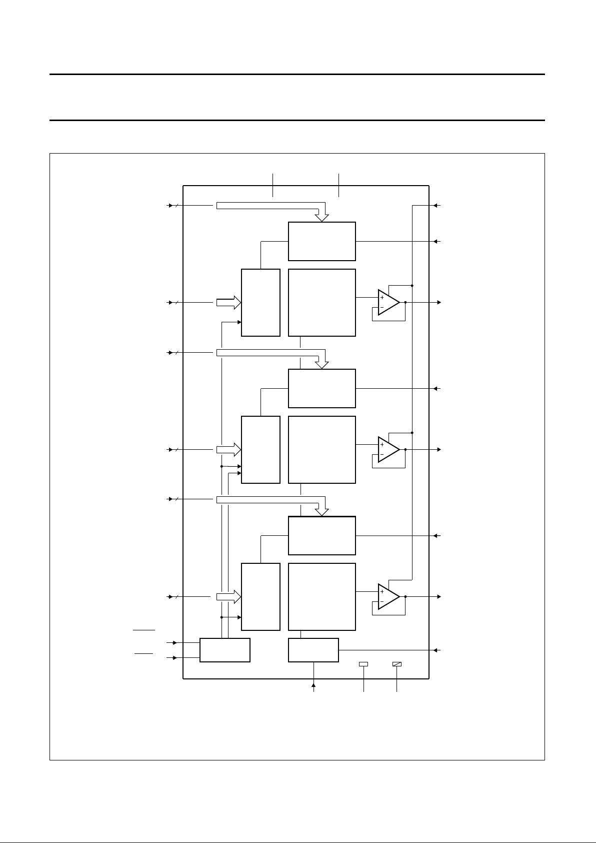
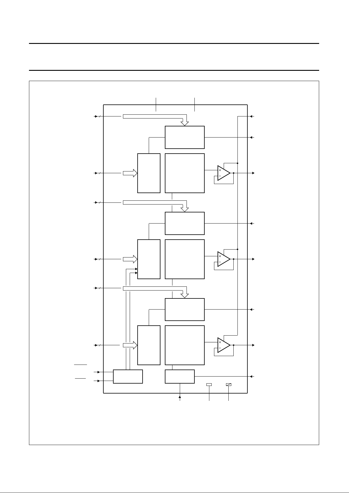
BLOCK DIAGRAMS
Fig.1 Block diagram for TDA8772.
handbook, full pagewidth
MBB661 - 2
RESISTOR
STRING
MSB
DECODER
LSB
DECODER
4
4
RESISTOR
STRING
MSB
DECODER
LSB
DECODER
4
4
RESISTOR
STRING
MSB
DECODER
LSB
DECODER
4
4
31–284
27–24
4
BANDGAP
REFERENCE
CONTROL
REGISTER
12
11
16–13
4
20–17
4
4–1
4
8–5
4
34
36
37,42 9,33
40
44
41
10,3235,39,43
V
DDA DDD
V
reference
current input
RED
analog output
GREEN
analog output
BLUE
analog output
V
SSA SSD
V
reference voltage
decoupling input
BLANK
control input
SYNC
control input
BLUE
digital inputs
(bits B4 to B7)
BLUE
digital inputs
(bits B0 to B3)
GREEN
digital inputs
(bits G4 to G7)
GREEN
digital inputs
(bits G0 to G3)
RED
digital inputs
(bits R4 to R7)
RED
digital inputs
(bits R0 to R3)
TDA8772
RED
clock input
GREEN
clock input
22
BLUE
clock input
23
reference current
input for internal
reference
21
38
(V )
REF
(I )
REFA
(I )
REFB
1995 Mar 09 5
Philips Semiconductors Product specification
Triple 8-bit video digital-to-analog
converter
TDA8772; TDA8772A
Fig.2 Block diagram for TDA8772A.
handbook, full pagewidth
MLB724
RESISTOR
STRING
MSB
DECODER
LSB
DECODER
4
4
RESISTOR
STRING
MSB
DECODER
LSB
DECODER
4
4
RESISTOR
STRING
MSB
DECODER
LSB
DECODER
4
4
31–284
27–24
4
BANDGAP
REFERENCE
CONTROL
REGISTER
12
11
16–13
4
20–17
4
4–1
4
8–5
4
34
36
37,42 9,33
40
44
41
10,3235,39,43
V
DDA DDD
V
reference
current input
RED
analog output
GREEN
analog output
BLUE
analog output
V
SSA SSD
V
reference voltage
decoupling input
BLANK
control input
SYNC
control input
BLUE
digital inputs
(bits B4 to B7)
BLUE
digital inputs
(bits B0 to B3)
GREEN
digital inputs
(bits G4 to G7)
GREEN
digital inputs
(bits G0 to G3)
RED
digital inputs
(bits R4 to R7)
RED
digital inputs
(bits R0 to R3)
TDA8772A
RED
clock input
GREEN
clock input
22
BLUE
clock input
23
reference current
input for internal
reference
21
38
(V )
REF
(I )
REFA
(I )
REFB
1995 Mar 09 6
Philips Semiconductors Product specification
Triple 8-bit video digital-to-analog
converter
TDA8772; TDA8772A
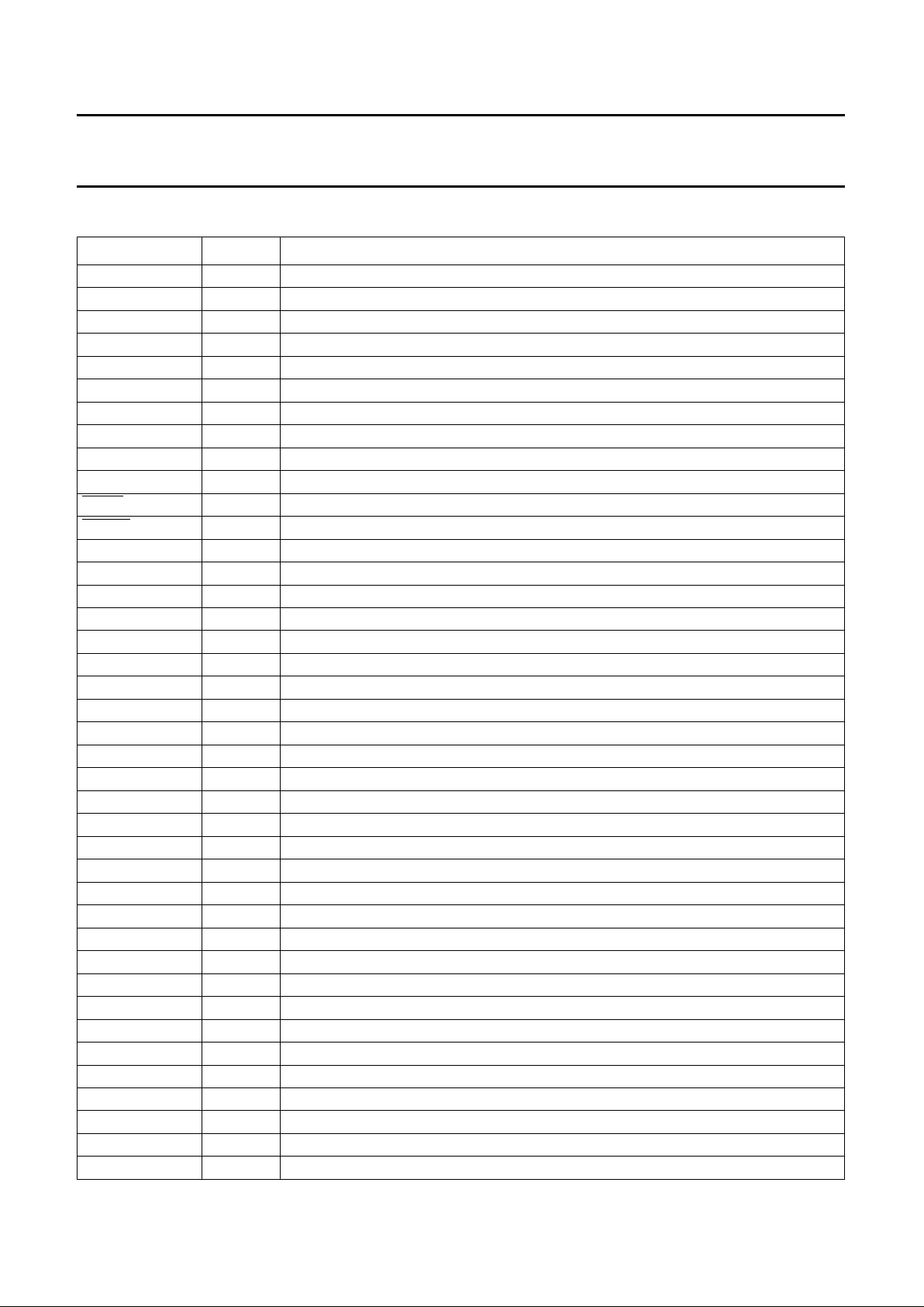
PINNING
SYMBOL PIN DESCRIPTION
R7 1 RED digital input data; bit 7 (MSB)
R6 2 RED digital input data; bit 6
R5 3 RED digital input data; bit 5
R4 4 RED digital input data; bit 4
R3 5 RED digital input data; bit 3
R2 6 RED digital input data; bit 2
R1 7 RED digital input data; bit 1
R0 8 RED digital input data; bit 0 (LSB)
V
SSD1
9 digital supply ground 1
V
DDD1
10 digital supply voltage 1
SYNC 11 composite sync control input; for GREEN channel only (active LOW)
BLANK 12 composite blank control input (active LOW)
G7 13 GREEN digital input data; bit 7 (MSB)
G6 14 GREEN digital input data; bit 6
G5 15 GREEN digital input data; bit 5
G4 16 GREEN digital input data; bit 4
G3 17 GREEN digital input data; bit 3
G2 18 GREEN digital input data; bit 2
G1 19 GREEN digital input data; bit 1
G0 20 GREEN digital input data; bit 0 (LSB)
CLKR 21 RED clock input
CLKG 22 GREEN clock input
CLKB 23 BLUE clock input
B7 24 BLUE digital input data; bit 7 (MSB)
B6 25 BLUE digital input data; bit 6
B5 26 BLUE digital input data; bit 5
B4 27 BLUE digital input data; bit 4
B3 28 BLUE digital input data; bit 3
B2 29 BLUE digital input data; bit 2
B1 30 BLUE digital input data; bit 1
B0 31 BLUE digital input data; bit 0 (LSB)
V
DDD2
32 digital supply voltage 2
V
SSD2
33 digital supply ground 2
V
REF
34 decoupling input for reference voltage
V
DDA1
35 analog supply voltage 1
OUTB 36 BLUE analog output
V
SSA1
37 analog supply ground 1
I
REFA
38 reference current input for internal reference
V
DDA2
39 analog supply voltage 2
OUTG 40 GREEN analog output
 Loading...