

Philips tda8771a DATASHEETS

INTEGRATED CIRCUITS
DATA SH EET
TDA8771A
Triple 8-bit video Digital-to-Analog
Converter (DAC)
Product specification
File under Integrated Circuits, IC02
1996 Jan 25
Philips Semiconductors Product specification
Triple 8-bit video Digital-to-Analog
Converter (DAC)
FEATURES
• 8-bit resolution
• Sampling rate up to 35 MHz
• Internal reference voltage regulator
• No deglitching circuit required
• Large output voltage range
• 1kΩ output load
• Power dissipation only 200 mW
• Single 5 V power supply
• 44-pin QFP package.
APPLICATIONS
• General purpose high-speed digital-to-analog
conversion
• Digital TV
• Graphic display
• Desktop video processing.
TDA8771A
GENERAL DESCRIPTION
The TDA8771A is a triple 8-bit video Digital-to-Analog
Converter (DAC). It converts the digital input signals into
analog voltage outputs at a maximum conversion rate of
35 MHz.
The DACs are based on resistor-string architecture with
integrated output buffers. The output voltage range is
determined by a built-in reference source.
The device is fabricated in a 5 V, CMOS process that
ensures high functionality with low power dissipation.
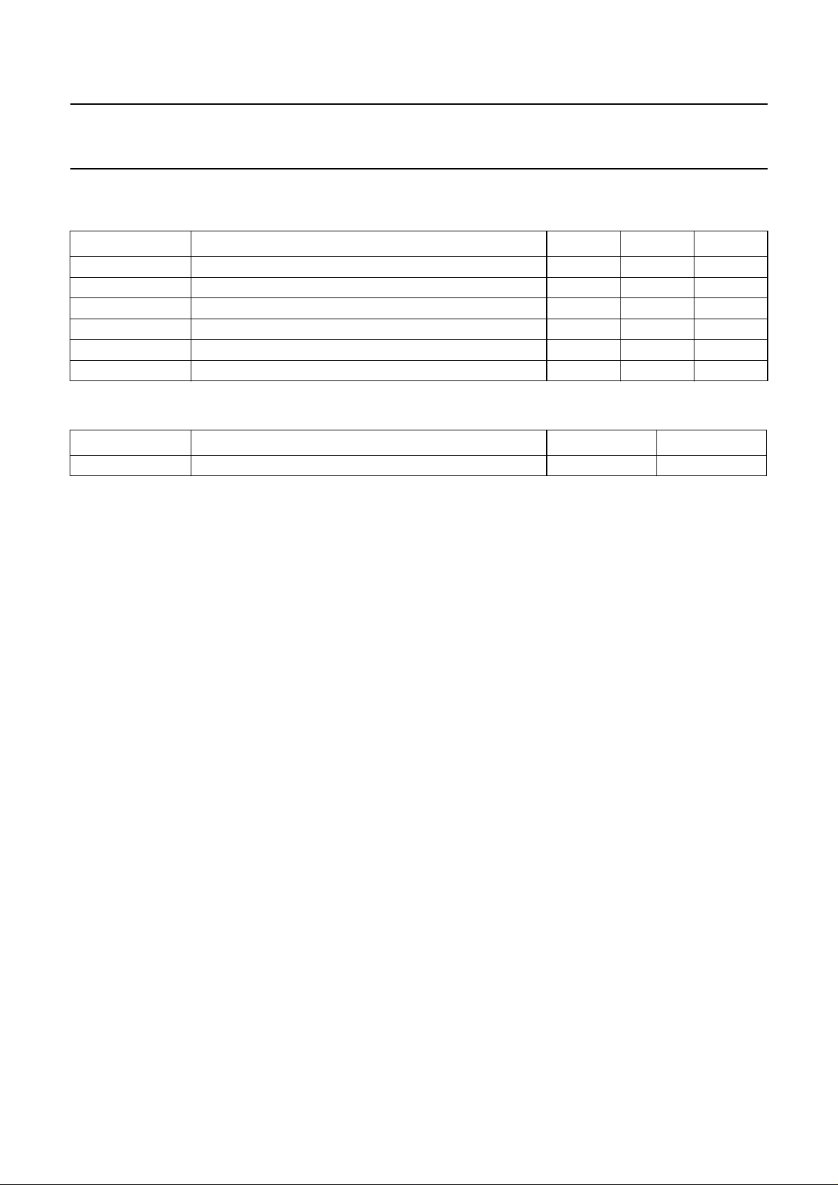
QUICK REFERENCE DATA
SYMBOL PARAMETER CONDITIONS MIN. TYP. MAX. UNIT
V
DDA
V
DDD
I
DDA
I
DDD
INL integral non-linearity f
DNL differential non-linearity f
f
clk(max)
P
tot
analog supply voltage 4.5 5.0 5.5 V
digital supply voltage 4.5 5.0 5.5 V
analog supply current RL=1kΩ; note 1 10 33 45 mA
digital supply current f
= 35 MHz − 720mA
clk
= 35 MHz; ramp input −±0.5 ±1 LSB
clk
= 35 MHz; ramp input −±0.25 ±0.5 LSB
clk
maximum clock frequency 35 −−MHz
total power dissipation RL=1kΩ; f
= 35 MHz; note 1 45 200 360 mW
clk
Note
1. Minimum and maximum data of current and power consumption are measured in worse case conditions: for
minimum data, all digital inputs are at logic level 0 while for maximum data, all digital inputs are at logic level 1.
ORDERING INFORMATION
TYPE
NUMBER
NAME DESCRIPTION VERSION
TDA8771AH QFP44 plastic quad flat package; 44 leads (lead length 1.3 mm);
P ACKAGE
SOT307-2
body 10 × 10 × 1.75 mm
1996 Jan 25 2
Philips Semiconductors Product specification
Triple 8-bit video Digital-to-Analog
Converter (DAC)
BLOCK DIAGRAM
handbook, full pagewidth
(bits R0 to R3)
(bits R4 to R7)
(bits G0 to G3)
RED
digital inputs
RED
digital inputs
GREEN
digital inputs
4
4
4
12 to 9
8
5 to 3
20 to 17
V
TDA8771A
4
DDA DDD
DECODER
MSB
V
7,2732,35,39,43
LSB
DECODER
RESISTOR
STRING
TDA8771A
clock input
31
4
4
1
44
reference
current input
(I )
REF
RED
analog output
GREEN
digital inputs
(bits G4 to G7)
BLUE
digital inputs
(bits B0 to B3)
BLUE
digital inputs
(bits B4 to B7)
4
16 to 13
4
30,29
26,25
4
24 to 21
34, 37, 38,41 33
4
4
MSB
DECODER
MSB
DECODER
LSB
DECODER
RESISTOR
STRING
4
LSB
DECODER
RESISTOR
STRING
BANDGAP
REFERENCE
2,42 6,28
40
36
GREEN
analog output
BLUE
analog output
MBH039
not
connected
reference voltage
decoupling input
Fig.1 Block diagram.
1996 Jan 25 3
(V )
REF
V
V
SSA SSD
Philips Semiconductors Product specification
Triple 8-bit video Digital-to-Analog
Converter (DAC)
PINNING
SYMBOL PIN DESCRIPTION
I
REF
V
SSA1
R7 3 RED digital input data; bit 7 (MSB)
R6 4 RED digital input data; bit 6
R5 5 RED digital input data; bit 5
V
SSD1
V
DDD1
R4 8 RED digital input data; bit 4
R3 9 RED digital input data; bit 3
R2 10 RED digital input data; bit 2
R1 11 RED digital input data; bit 1
R0 12 RED digital input data; bit 0 (LSB)
G7 13 GREEN digital input data; bit 7 (MSB)
G6 14 GREEN digital input data; bit 6
G5 15 GREEN digital input data; bit 5
G4 16 GREEN digital input data; bit 4
G3 17 GREEN digital input data; bit 3
G2 18 GREEN digital input data; bit 2
G1 19 GREEN digital input data; bit 1
G0 20 GREEN digital input data; bit 0 (LSB)
B7 21 BLUE digital input data; bit 7 (MSB)
B6 22 BLUE digital input data; bit 6
B5 23 BLUE digital input data; bit 5
B4 24 BLUE digital input data; bit 4
B3 25 BLUE digital input data; bit 3
B2 26 BLUE digital input data; bit 2
V
DDD2
V
SSD2
B1 29 BLUE digital input data; bit 1
B0 30 BLUE digital input data; bit 0 (LSB)
CLK 31 clock input
V
DDA1
V
REF
n.c. 34 not connected
V
DDA2
OUTB 36 BLUE analog output
n.c. 37 not connected
n.c. 38 not connected
V
DDA3
OUTG 40 GREEN analog output
1 reference current input for output buffers
2 analog supply ground 1
6 digital supply ground 1
7 digital supply voltage 1
27 digital supply voltage 2
28 digital supply ground 2
32 analog supply voltage 1
33 decoupling input for reference voltage
35 analog supply voltage 2
39 analog supply voltage 3
TDA8771A
1996 Jan 25 4
Philips Semiconductors Product specification
Triple 8-bit video Digital-to-Analog
Converter (DAC)
SYMBOL PIN DESCRIPTION
n.c. 41 not connected
V
SSA2
V
DDA4
OUTR 44 RED analog output
handbook, full pagewidth
42 analog supply ground 2
43 analog supply voltage 4
OUTR
I
V
SSA1
V
SSD1
V
DDD1
REF
R7
R6
R5
R4
R3
R2
R1
index
corner
1
2
3
4
5
6
7
8
9
10
11
44
DDA4
V
43
SSA2
V
42
OUTG
n.c.
41
40
TDA8771A
DDA3
V
39
n.c.
38
n.c.
37
OUTB
36
V
DDA2
35
n.c.
34
TDA8771A
V
33
REF
V
32
DDA1
31
CLK
30
B0
29
B1
V
28
SSD2
V
27
DDD2
26
B2
B3
25
24
B4
23
B5
12
13
14
15
16
R0
G7
G4G3G2G1G0
G6
G5
Fig.2 Pin configuration.
1996 Jan 25 5
20
21
B7
22
B6
MBH040
17
18
19
Philips Semiconductors Product specification
Triple 8-bit video Digital-to-Analog
TDA8771A
Converter (DAC)
LIMITING VALUES
In accordance with the Absolute Maximum Rating System (IEC134).
SYMBOL PARAMETER MIN. MAX. UNIT
V
DDA
V
DDD
∆V
DD
T
stg
T
amb
T
j
THERMAL CHARACTERISTICS
SYMBOL PARAMETER VALUE UNIT
R
th j-a
HANDLING
Inputs and outputs are protected against electrostatic discharges in normal handling. However, to be totally safe, it is
desirable to take normal precautions appropriate to handling integrated circuits.
analog supply voltage −0.5 +6.5 V
digital supply voltage −0.5 +6.5 V
supply voltage difference between V
DDA
and V
DDD
−1.0 +1.0 V
storage temperature −55 +150 °C
operating ambient temperature 0 +70 °C
junction temperature − +125 °C
thermal resistance from junction to ambient in free air 75 K/W
1996 Jan 25 6
 Loading...