

Philips TDA8766G Datasheet

INTEGRATED CIRCUITS
DATA SH EET
TDA8766
10-bit high-speed 3.0 to 5.25 V
analog-to-digital converter
Product specification
Supersedes data of 2000 May 25
File under Integrated Circuits, IC02
2001 Apr 19
Philips Semiconductors Product specification
10-bit high-speed 3.0 to 5.25 V
analog-to-digital converter
FEATURES
• 10-bit resolution
• 3.0 to 5.25 V operation
• Sampling rate up to 20 MHz
• DC sampling allowed
• High signal-to-noise ratio over a large analog input
frequency range(9.3 effective bits at 1.0 MHz; full-scale
input at f
• In-Range (IR) CMOS output
• CMOS/TTL compatible digital inputs and outputs
• External reference voltage regulator
• Power dissipation only 53 mW (typical value)
• Low analog input capacitance, no buffer amplifier
required
• Standby mode
• No sample-and-hold circuit required.
= 20 MHz)
clk
TDA8766
APPLICATIONS
High-speed analog-to-digital conversion for:
• Video data digitizing
• Camera
• Camcorder
• Radio communication.
GENERAL DESCRIPTION
The TDA8766 is a 10-bit high-speed Analog-to-Digital
Converter (ADC) for professional video and other
applications. It converts with 3.0 to 5.25 V operation the
analoginput signalinto10-bit binary-codeddigitalwords at
a maximumsampling rateof 20 MHz. Alldigital inputs and
outputs are CMOS compatible. A standby mode allows
reduction ofthe devicepower consumptiondown to 4 mW.
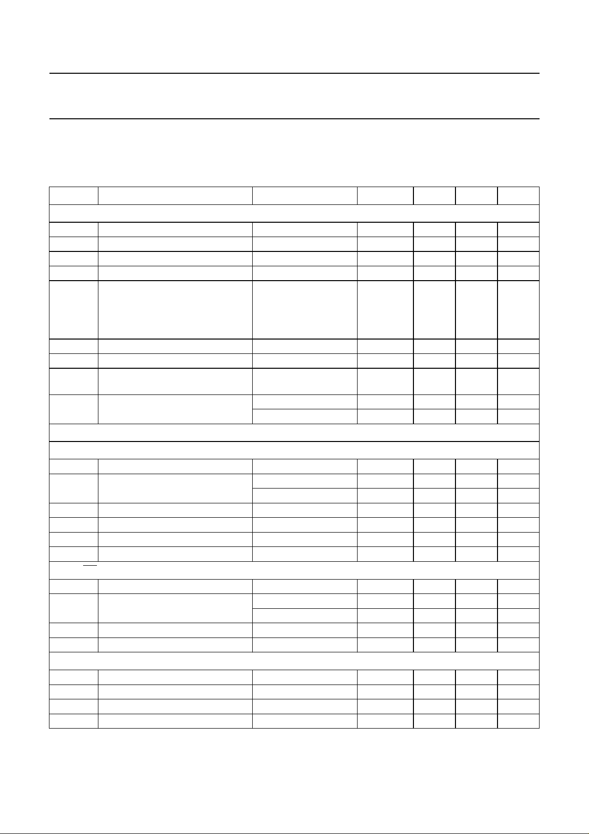
QUICK REFERENCE DATA
SYMBOL PARAMETER CONDITIONS MIN. TYP. MAX. UNIT
V
V
V
V
I
DDA
I
DDD
I
DDO
DDA
DDD1
DDD2
DDO
analog supply voltage 3.0 3.3 5.25 V
digital supply voltage 1 3.0 3.3 5.25 V
digital supply voltage 2 3.0 3.3 5.25 V
output stages supply voltage 3.0 3.3 5.25 V
analog supply current − 7.5 10 mA
digital supply current − 7.5 10 mA
output stages supply current f
= 20 MHz; CL= 20 pF; ramp
clk
− 12mA
input
INL integral non-linearity f
DNL differential non-linearity f
f
clk(max)
P
tot
maximum clock frequency 20 −−MHz
total power dissipation V
= 20 MHz; ramp input −±1±2 LSB
clk
= 20 MHz; ramp input −±0.25 ±0.7 LSB
clk
DDA=VDDD=VDDO
= 3.3 V − 53 73 mW
ORDERING INFORMATION
TYPE
NUMBER
NAME DESCRIPTION VERSION
PACKAGE
TDA8766G LQFP32 plastic low profile quad flat package; 32 leads; body 5 × 5 × 1.4 mm SOT401-1
2001 Apr 19 2
Philips Semiconductors Product specification
10-bit high-speed 3.0 to 5.25 V
analog-to-digital converter
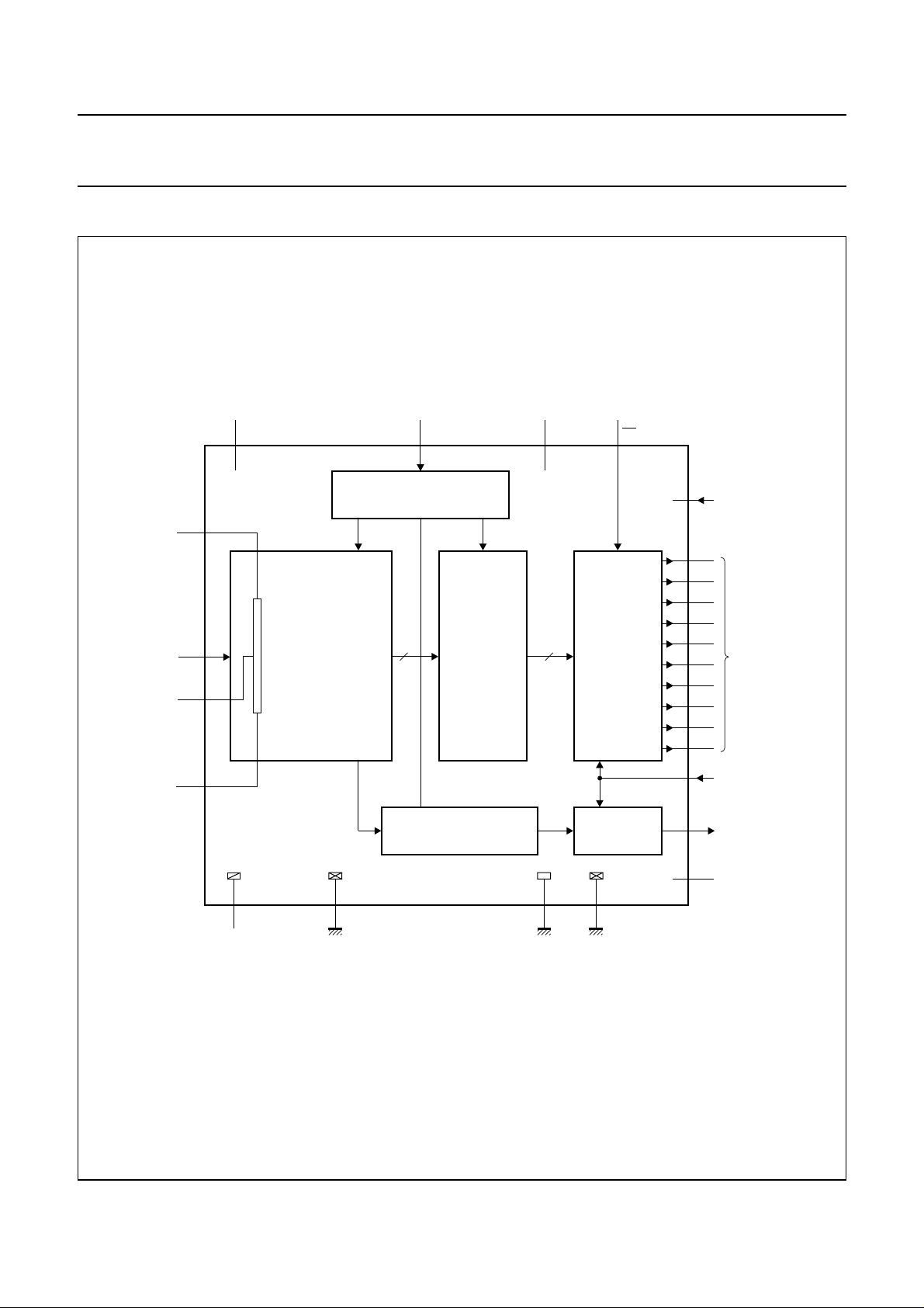
BLOCK DIAGRAM
handbook, full pagewidth
analog
voltage input
V
RT
V
V
RM
V
DDA
7
15
R
LAD
I
14
11
ANALOG -TO - DIGITAL
CONVERTER
CLK
5
CLOCK DRIVER
LATCHES
V
DDD2
18
TDA8766
OE
16
CMOS
OUTPUTS
6
1
D9
D8
31
D7
30
D6
29
D5
28
27 D4
26
D3
25
D2
23 D1
22
D0
TDA8766
STDBY
MSB
data outputs
LSB
V
10
RB
IN-RANGE LATCH
9
V
analog
ground
SSA
19
V
digital
ground 2
SSD2
Fig.1 Block diagram.
2001 Apr 19 3
V
SSOVSSD1
output
ground
CMOS
OUTPUT
321
digital
ground 1
20
MLC853
V
DDO
2
4
IR output
V
DDD1
Philips Semiconductors Product specification
10-bit high-speed 3.0 to 5.25 V
analog-to-digital converter
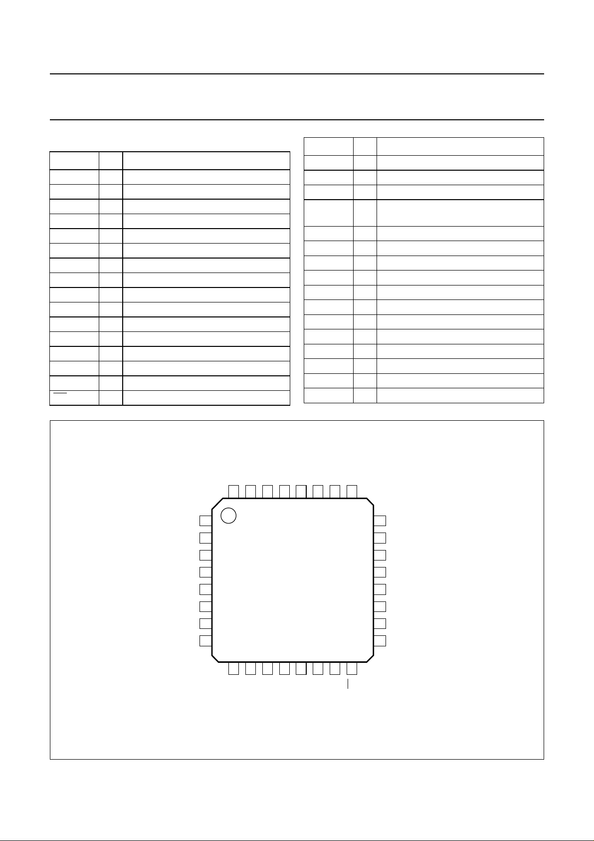
PINNING
SYMBOL PIN DESCRIPTION
D9 1 data output; bit 9 (MSB)
IR 2 in-range data output
V
SSD1
V
DDD1
CLK 5 clock input
STDBY 6 standby mode input
V
DDA
n.c. 8 not connected
V
SSA
V
RB
V
RM
n.c. 12 not connected
n.c. 13 not connected
V
I
V
RT
OE 16 output enable input (active LOW)
3 digital ground 1
4 digital supply voltage 1 (3.0 to 5.25 V)
7 analog supply voltage (3.0 to 5.25 V)
9 analog ground
10 reference voltage BOTTOM input
11 reference voltage MIDDLE input
14 analog voltage input
15 reference voltage TOP input
TDA8766
SYMBOL PIN DESCRIPTION
n.c. 17 not connected
V
DDD2
V
SSD2
V
DDO
V
SSO
D0 22 data output; bit 0 (LSB)
D1 23 data output; bit 1
n.c. 24 not connected
D2 25 data output; bit 2
D3 26 data output; bit 3
D4 27 data output; bit 4
D5 28 data output; bit 5
D6 29 data output; bit 6
D7 30 data output; bit 7
D8 31 data output; bit 8
n.c. 32 not connected
18 digital supply voltage 2 (3.0 to 5.25 V)
19 digital ground 2
20 positive supply voltage for
output stage (3.0 to 5.25 V)
21 output stage ground
handbook, full pagewidth
D9
V
SSD1
V
DDD1
CLK
STDBY
V
DDA
n.c.
n.c.
D8
D7
D6
D5
D4
D3
D2
32
31
30
29
28
27
26
25
1
2
IR
3
4
TDA8766
5
6
7
8
9
10
11
12
13
14
15
16
RT
OE
V
SSA
V
I
RB
RM
V
n.c.
V
n.c.
V
24
23
22
21
20
19
18
17
MLC854
n.c.
D1
D0
V
SSO
V
DDO
V
SSD2
V
DDD2
n.c.
Fig.2 Pin configuration.
2001 Apr 19 4
Philips Semiconductors Product specification
10-bit high-speed 3.0 to 5.25 V
TDA8766
analog-to-digital converter
LIMITING VALUES
In accordance with the Absolute Maximum Rating System (IEC 60134).
SYMBOL PARAMETER CONDITIONS MIN. MAX. UNIT
V
V
V
∆V
V
V
I
O
T
T
T
DDA
DDD
DDO
DD
I
i(p-p)
stg
amb
j
analog supply voltage note 1 −0.3 +7.0 V
digital supply voltage note 1 −0.3 +7.0 V
output stages supply voltage note 1 −0.3 +7.0 V
supply voltage difference
V
− V
V
V
DDA
DDD
DDA
− V
− V
DDD
DDO
DDO
input voltage referenced to V
AC input voltage for switching
referenced to V
SSA
SSD
−1.0 +4.0 V
−1.0 +4.0 V
−1.0 +4.0 V
−0.3 +7.0 V
− V
DDD
(peak-to-peak value)
output current − 10 mA
storage temperature −55 +150 °C
ambient temperature −20 +75 °C
junction temperature − 150 °C
V
Note
1. The supply voltages V
DDA
, V
DDD
and V
may have any value between −0.3 and +7.0 V provided that the supply
DDO
voltage differences ∆VDD are respected.
HANDLING
Inputs and outputs are protected against electrostatic discharges in normal handling. However, to be totally safe, it is
desirable to take normal precautions appropriate to handling integrated circuits.
THERMAL CHARACTERISTICS
SYMBOL PARAMETER CONDITIONS VALUE UNIT
R
th(jj-a)
thermal resistance from junction to ambient in free air 90 K/W
2001 Apr 19 5
Philips Semiconductors Product specification
10-bit high-speed 3.0 to 5.25 V
TDA8766
analog-to-digital converter
CHARACTERISTICS
V
DDA=V7
short-circuited together; V
otherwise specified.
SYMBOL PARAMETER CONDITIONS MIN. TYP. MAX. UNIT
Supplies
V
DDA
V
DDD1
V
DDD2
V
DDO
∆V
I
DDA
I
DDD
I
DDO
P
tot
Inputs
DD
to V9= 3.3 V; V
DDD=V4
i(p-p)
to V3=V18to V19= 3.3 V; V
= 1.83 V;CL= 20 pF; T
DDO=V20
= 0 to 70 °C; typicalvalues measured at T
amb
to V21= 3.3 V; V
SSA,VSSD
and V
SSO
=25°C; unless
amb
analog supply voltage 3.0 3.3 5.25 V
digital supply voltage 1 3.0 3.3 5.25 V
digital supply voltage 2 3.0 3.3 5.25 V
output stages supply voltage 3.0 3.3 5.25 V
voltage difference
V
V
V
DDA
DDA
DDD
− V
− V
− V
DDD
DDO
DDO
−0.2 − +0.2 V
−0.2 − +2.25 V
−0.2 − +2.25 V
analog supply current − 7.5 10 mA
digital supply current − 7.5 10 mA
output stages supply current f
= 20 MHz;
clk
− 12mA
ramp input; CL=20pF
total power dissipation operating; VDD= 3.3 V − 53 73 mW
standby mode − 4 − mW
C
LOCK INPUT CLK (REFERENCED TO V
V
IL
V
IH
I
IL
I
IH
Z
i
C
i
LOW-level input voltage 0 − 0.3V
HIGH-level input voltage V
LOW-level input current V
HIGH-level input current V
input impedance f
input capacitance f
SSD
); note 1
INPUTS OE AND STDBY (REFERENCED TO V
V
IL
V
IH
I
IL
I
IH
ANALOG INPUT VI(REFERENCED TO V
I
IL
I
IH
Z
i
C
i
LOW-level input voltage 0 − 0.3V
HIGH-level input voltage V
LOW-level input current VIL= 0.3 V
HIGH-level input current VIH= 0.7 V
)
SSA
LOW-level input current VI=V
HIGH-level input current VI=V
input impedance fi= 1 MHz − 5 − kΩ
input capacitance fi= 1 MHz − 8 − pF
≤ 3.6 V 0.6V
DDD
V
= 3.3 V 0.7V
DDD
= 0.3V
CLK
= 0.7V
CLK
= 20 MHz − 4 − kΩ
clk
= 20 MHz − 3 − pF
clk
); see Tables 1 and 2
SSD
≤ 3.6 V 0.6V
DDD
V
= 3.3 V 0.7V
DDD
RB
RT
DDD
DDD
DDD
DDD
V
DDD
DDD
DDD
− V
− V
DDD
DDD
V
V
−10+1µA
−−5µA
V
DDD
DDD
DDD
− V
− V
DDD
DDD
V
V
−1 −−µA
−−1µA
− 0 −µA
− 35 −µA
2001 Apr 19 6
Philips Semiconductors Product specification
10-bit high-speed 3.0 to 5.25 V
TDA8766
analog-to-digital converter
SYMBOL PARAMETER CONDITIONS MIN. TYP. MAX. UNIT
Reference voltages for resistor ladder; see Table 3
V
RB
V
RT
V
diff(ref)
I
ref
R
LAD
TC
RLAD
V
offset(B)
V
offset(T)
V
I(p-p)
Outputs
DIGITAL OUTPUTS D9 TO D0 AND IR (REFERENCED TO V
V
OL
V
OH
I
OZ
Switching characteristics
reference voltage BOTTOM 1.1 1.2 − V
reference voltage TOP 3.0 3.3 V
differential reference voltage
VRT− V
RB
1.9 2.1 3.0 V
DDA
V
reference current − 7.2 − mA
ladder resistance − 290 −Ω
temperature coefficient of ladder
resistance
− 539 − mΩ/K
− 1860 − ppm
offset voltage BOTTOM note 2 − 135 − mV
offset voltage TOP note 2 − 135 − mV
analog input voltage
note 3 1.66 1.83 2.35 V
(peak-to-peak value)
)
SSD
LOW-level output voltage IO=1mA 0 − 0.5 V
HIGH-level output voltage IO= −1mA V
output current in 3-state mode 0.5 V < VO<V
DDO
− 0.5 − V
DDO
DDO
V
−20 −+20 µA
CLOCK INPUT CLK; see Fig.4; note 1
f
clk(max)
t
CPH
t
CPL
Analog signal processing (f
L
INEARITY
maximum clock frequency 20 −−MHz
clock pulse width HIGH 15 −−ns
clock pulse width LOW 15 −−ns
= 20 MHz)
clk
INL integral non-linearity ramp input; see Fig.6 −±1±2 LSB
DNL differential non-linearity ramp input; see Fig.7 −±0.25 ±0.7 LSB
I
NPUT SET RESPONSE; see Fig.8; note 4
t
STLH
analog input settling time
full-scale square wave − 46ns
LOW-to-HIGH
t
STHL
analog input settling time
full-scale square wave − 46ns
HIGH-to-LOW
HARMONICS; see Fig.9; note 5
THD total harmonic distortion f
= 1 MHz −−63 − dB
i
SIGNAL-TO-NOISE RATIO; see Fig.9; note 5
S/N signal-to-noise ratio (full-scale) without harmonics;
= 1 MHz
f
i
− 60 − dB
2001 Apr 19 7
Philips Semiconductors Product specification
10-bit high-speed 3.0 to 5.25 V
TDA8766
analog-to-digital converter
SYMBOL PARAMETER CONDITIONS MIN. TYP. MAX. UNIT
E
FFECTIVE BITS; see Fig.9; note 5
EB effective bits f
Timing (f
t
ds
t
h
t
d
= 20 MHz; CL= 20 pF); see Fig.4; note 6
clk
sampling delay time −−5ns
output hold time 5 −−ns
output delay time V
3-state output delay times; see Fig.5
t
dZH
t
dZL
t
dHZ
t
dLZ
enable HIGH − 14 18 ns
enable LOW − 16 20 ns
disable HIGH − 16 20 ns
disable LOW − 14 18 ns
Standby mode output delay times
t
d(stb)LH
t
d(stb)HL
standby LOW-to-HIGH transition −−200 ns
start-up HIGH-to-LOW transition −−500 ns
Notes
1. In additionto agood layoutof thedigital andanalog ground,it isrecommended thatthe riseand falltimes ofthe clock
must not be less than 1 ns.
2. Analog input voltages producing code 0 up to and including 1023:
a) V
(offset voltage BOTTOM) is the difference between the analog input which produces data equal to 00
offset(B)
and the reference voltage BOTTOM (VRB) at T
b) V
(offset voltage TOP) is the difference between VRT(reference voltage TOP) and the analog input which
offset(T)
produces data outputs equal to 1023 at T
3. In orderto ensure theoptimum linearity performanceof such converterarchitecture, the lowerand upper extremities
of theconverter reference resistorladder (corresponding tooutput codes 0 and 1023 respectively) areconnected to
pins VRB and VRT via offset resistors ROB and ROT as shown in Fig.3.
= 300 kHz − 9.5 − bits
i
f
= 1 MHz − 9.3 − bits
i
f
= 3.58 MHz − 8.0 − bits
i
= 4.75 V 8 12 15 ns
DDO
V
= 3.15 V 8 17 20 ns
DDO
=25°C.
amb
=25°C.
amb
a) Thecurrentflowing intothe resistorladderis andthe full-scaleinput range atthe converter,
to cover code 0 to code 1023, is
V
I
RLIL×
I
L
VRTVRB–
=
------------------------------------------
++
R
OBRLROT
R
-----------------------------------------R
L
++
OBRLROT
–()0.871 V
V
RTVRB
–()×=×==
RTVRB
b) Since RL, ROBand ROT have similar behaviour with respect to process and temperature variation, the ratio
R
----------------------------------------R
L
++
OBRLROT
codes ata giveninput voltage depends mainly onthe differenceV
will be kept reasonably constant from device to device. Consequently variation of the output
− VRBand itsvariation withtemperature and
RT
supply voltage. When several ADCs are connected in parallel and fed with the same reference source, the
matching between each of them is then optimized.
4. The analoginput settlingtime isthe minimum time required forthe inputsignal tobe stabilized aftera sharpfull-scale
input change (square-wave signal) in order to sample the signal and obtain correct output data.
2001 Apr 19 8
 Loading...