

Philips tda8764a DATASHEETS

INTEGRATED CIRCUITS
DATA SH EET
TDA8764A
10-bit high-speed low-power ADC
Product specification
File under Integrated Circuits, IC11
2000 Jul 03
Philips Semiconductors Product specification
10-bit high-speed low-power ADC TDA8764A
FEATURES
• 10-bit resolution (binary or gray code)
• Sampling rate up to 60 MHz
• DC sampling allowed
• One clock cycle conversion only
• High signal-to-noise ratio over a large analog input
frequency range (9.3 effective bits at 5 MHz full-scale
input at f
= 60 MHz)
clk
• No missing codes guaranteed
• In Range (IR) CMOS output
• TTL and CMOS levels compatible digital inputs
• 2.7 to 3.6 V CMOS digital outputs
• Low-level AC clock input signal allowed
• Power dissipation only 312 mW
• Low analog input capacitance, no buffer amplifier
required
• No sample-and-hold circuit required.
ORDERING INFORMATION
APPLICATIONS
High-speed analog-to-digital conversion for:
• Video data digitizing
• Radar pulse analysis
• High energy physics research
• Transient signal analysis
•Σ∆modulators
• Medical imaging.
GENERAL DESCRIPTION
The TDA8764A is a 10-bit high-speed low-power
Analog-to-Digital Converter (ADC) for professional video
and other applications. It converts the analog input signal
into10-bitbinaryorgraycodeddigitalwordsatamaximum
sampling rate of 60 MHz. All digital inputs and outputs are
TTL and CMOS compatible, although a low-level sine
wave clock input signal is allowed.
The device requires an external source to drive its
reference ladder.
TYPE NUMBER
PACKAGE
NAME DESCRIPTION VERSION
TDA8764ATS/6 SSOP28 plastic shrink small outline package; 28 leads; body width 5.3 mm SOT341-1
TDA8764AHL/6 LQFP32 plastic low profile quad flat package; 32 leads; body 5 × 5 × 1.4 mm SOT401-1
QUICK REFERENCE DATA
SYMBOL PARAMETER CONDITIONS MIN. TYP. MAX. UNIT
V
CCA
V
CCD
V
CCO
I
CCA
I
CCD
I
CCO
INL integral non-linearity f
DNL differential non-linearity f
f
clk(max)
analog supply voltage 4.75 5.0 5.25 V
digital supply voltage 4.75 5.0 5.25 V
output stages supply voltage 2.7 3.3 3.6 V
analog supply current − 29 37 mA
digital supply current − 33 40 mA
output stages supply current f
maximum clock frequency TDA8764ATS and
= 60 MHz; ramp input − 0.5 2.0 mA
clk
= 60 MHz; ramp input −±0.8 ±2 LSB
clk
= 60 MHz; ramp input −±0.35 ±0.9 LSB
clk
60 −−MHz
TDA8764AHL
P
tot
total power dissipation f
= 60 MHz; ramp input − 312 411 mW
clk
2000 Jul 03 2
Philips Semiconductors Product specification
10-bit high-speed low-power ADC TDA8764A
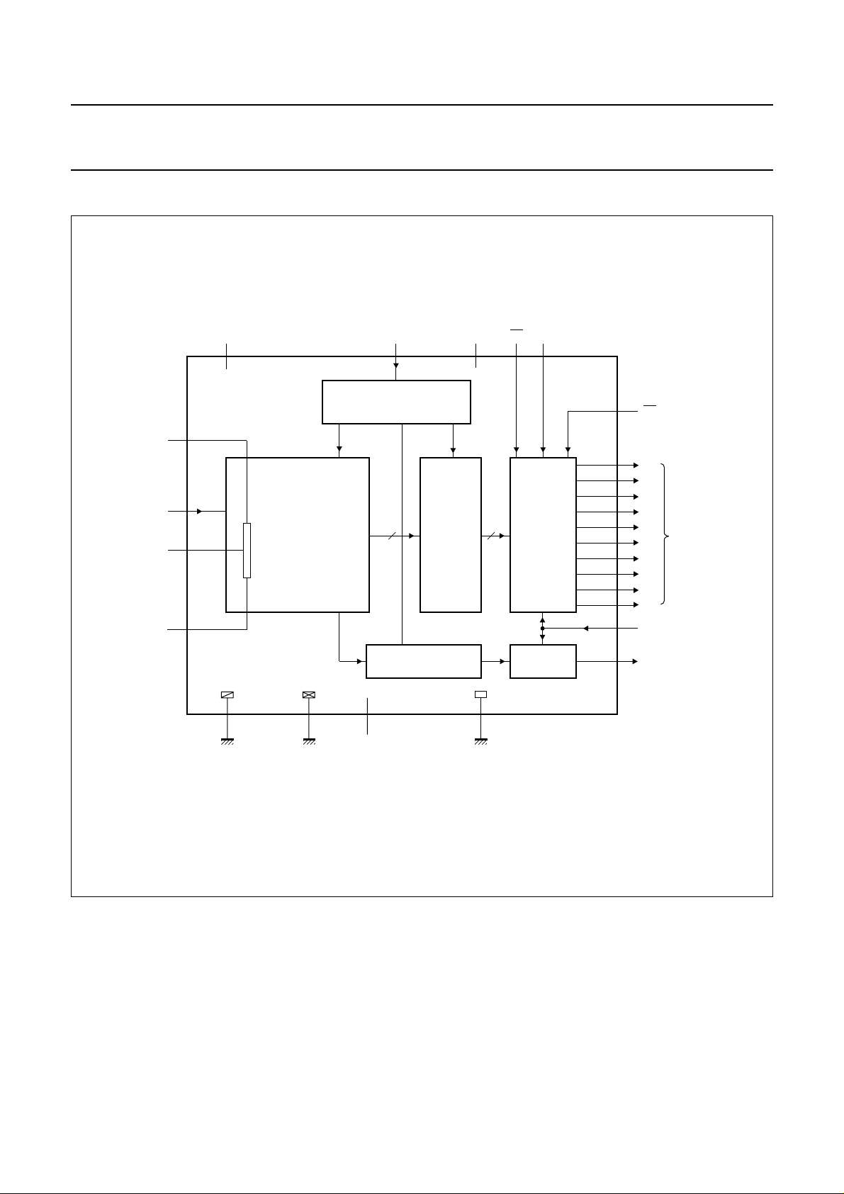
BLOCK DIAGRAM
handbook, full pagewidth
V
RT
analog
voltage input
V
RM
V
RB
V
CCA
3 (7) 1 (5) 10
9 (15)
V
8 (14)
I
7 (13)
6 (12)
ANALOG-TO-DIGITAL
CONVERTER
R
LAD
TDA8764A
4 (8) 12 (18)
AGND
DGND n.c.
CLK
CLOCK DRIVER
IN-RANGE LATCH
5, 27, 28
(9, 1, 3, 4, 10, 11, 32)
V
LATCHES
CCD
14 (20)
OGND
GRAY
OE
(16)
CMOS
OUTPUTS
CMOS
OUTPUT
15 (21)11 (17)
(6) 2
(31) 25
(30) 24
(29) 23
(28) 22
(27) 21
(26) 20
(25) 19
(24) 18
(23) 17
(22) 16
(19) 13
(2) 26
FCE253
TC
D9
MSB
D8
D7
D6
D5
D4
D3
D2
D1
LSB
D0
V
CCO
IR output
data outputs
The pin numbers given in parenthesis refer to the TDA8764AHL.
Fig.1 Block diagram.
2000 Jul 03 3
Philips Semiconductors Product specification
10-bit high-speed low-power ADC TDA8764A
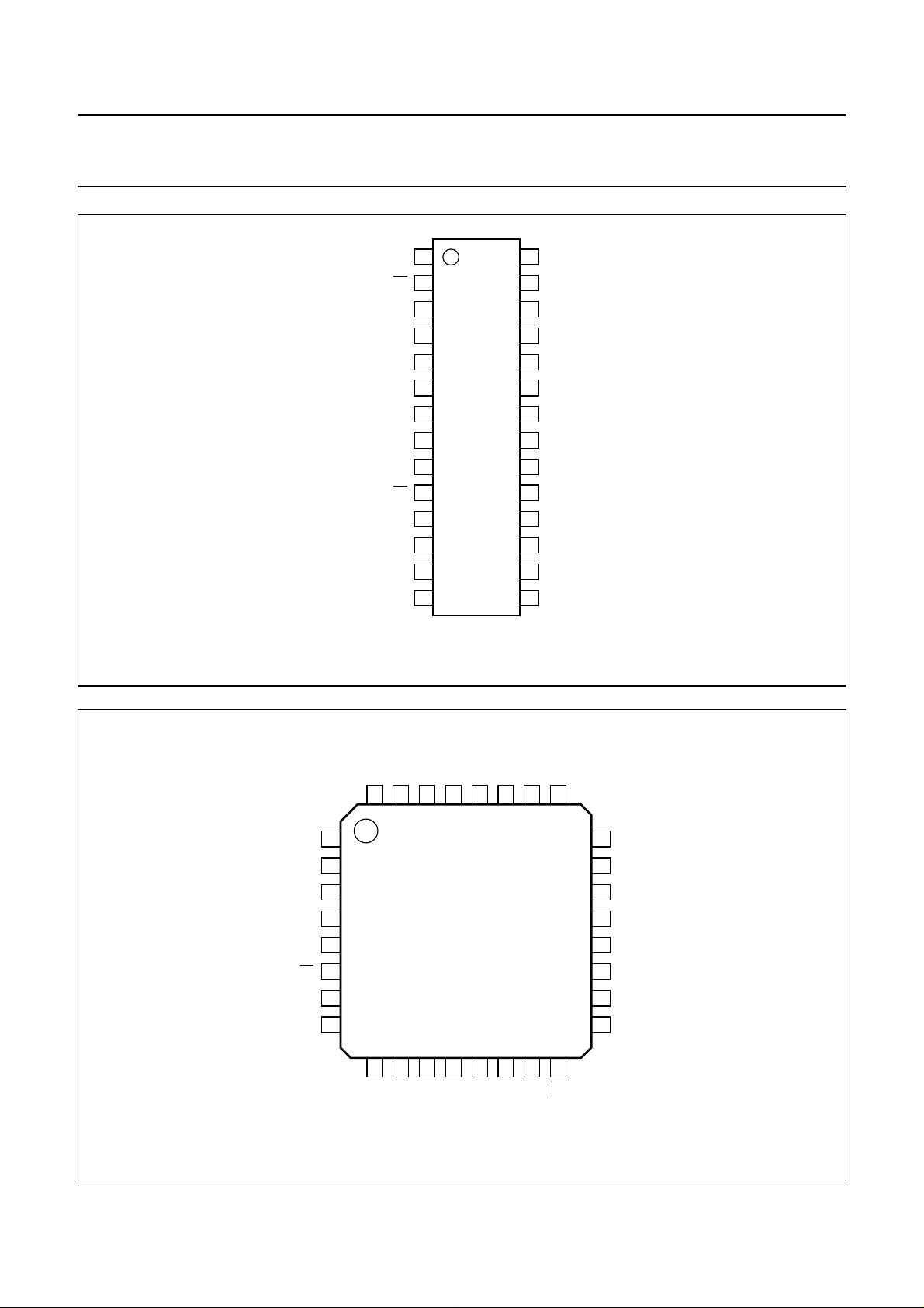
PINNING
SYMBOL
DESCRIPTION
TDA8764ATS TDA8764AHL
CLK 1 5 clock input
TC 2 6 twos complement input (active LOW)
PIN
V
CCA
3 7 analog supply voltage (5 V)
AGND 4 8 analog ground
n.c. 5 9 not connected
V
RB
V
RM
V
I
V
RT
6 12 reference voltage BOTTOM input
7 13 reference voltage MIDDLE input
8 14 analog input voltage
9 15 reference voltage TOP input
OE 10 16 output enable input (active LOW)
V
CCD
11 17 digital supply voltage (5 V)
DGND 12 18 digital ground
V
CCO
13 19 supply voltage for output stages (2.7 to 3.6 V)
OGND 14 20 output ground
GRAY 15 21 gray code input (active HIGH)
D0 16 22 data output; bit 0 (LSB)
D1 17 23 data output; bit 1
D2 18 24 data output; bit 2
D3 19 25 data output; bit 3
D4 20 26 data output; bit 4
D5 21 27 data output; bit 5
D6 22 28 data output; bit 6
D7 23 29 data output; bit 7
D8 24 30 data output; bit 8
D9 25 31 data output; bit 9 (MSB)
IR 26 2 in range data output
n.c. 27 1 not connected
n.c. 28 3 not connected
n.c. − 4 not connected
n.c. − 10 not connected
n.c. − 11 not connected
n.c. − 32 not connected
2000 Jul 03 4
Philips Semiconductors Product specification
10-bit high-speed low-power ADC TDA8764A
handbook, halfpage
Fig.2 Pin configuration (SSOP28).
CLK
TC
V
CCA
AGND
n.c.
V
RB
V
RM
V
RT
OE
V
CCD
DGND
V
CCO
OGND
1
2
3
4
5
6
7
V
8
I
9
10
11
12
13
TDA8764ATS
FCE254
n.c.
28
27
n.c.
IR
26
25
D9
24
D8
23
D7
22
D6
D5
21
20
D4
D3
19
D2
18
D1
17
D0
16
GRAY
1514
handbook, full pagewidth
n.c.
n.c.
n.c.
CLK
TC
V
CCA
AGND
n.c.
32
1
IR
2
3
4
5
6
7
8
9
n.c.
D8
D9
31
30
TDA8764AHL
10
11
n.c.
n.c.
Fig.3 Pin configuration (LQFP32).
2000 Jul 03 5
D7
29
12
RB
V
V
D6
28
13
RM
D5
D4
D3
27
26
25
D2
24
D1
23
22
D0
GRAY
21
20
OGND
V
19
CCO
18
DGND
V
17
CCD
14
15
I
V
RT
V
16
OE
FCE255
Philips Semiconductors Product specification
10-bit high-speed low-power ADC TDA8764A
LIMITING VALUES
In accordance with the Absolute Maximum Rating System (IEC 60134).
SYMBOL PARAMETER CONDITIONS MIN. MAX. UNIT
V
CCA
V
CCD
V
CCO
∆V
CC
V
I
V
i(sw)(p-p)
I
O
T
stg
T
amb
T
j
analog supply voltage note 1 −0.3 +7.0 V
digital supply voltage note 1 −0.3 +7.0 V
output stages supply voltage note 1 −0.3 +7.0 V
supply voltage difference between
V
V
V
CCA
CCA
CCD
− V
− V
− V
CCD
CCO
CCO
−1.0 +1.0 V
−1.0 +4.0 V
−1.0 +4.0 V
input voltage referenced to AGND −0.3 +7.0 V
AC input voltage for switching (peak-to-peak value) referenced to DGND − V
CCD
V
output current − 10 mA
storage temperature −55 +150 °C
ambient temperature −40 +85 °C
junction temperature − 150 °C
Note
1. The supply voltages V
CCA
, V
CCD
and V
may have any value between −0.3 and +7.0 V provided that the supply
CCO
voltage differences ∆VCC are respected.
HANDLING
Inputs and outputs are protected against electrostatic discharges in normal handling. However, to be totally safe, it is
desirable to take normal precautions appropriate to handling integrated circuits.
THERMAL CHARACTERISTICS
SYMBOL PARAMETER CONDITIONS VALUE UNIT
R
th(j-a)
thermal resistance from junction to ambient in free air
SSOP28 110 K/W
LQFP32 90 K/W
2000 Jul 03 6
Philips Semiconductors Product specification
10-bit high-speed low-power ADC TDA8764A
CHARACTERISTICS
V
= 4.75 to 5.25 V; V
CCA
T
= 0 to 70 °C; typical values measured at V
amb
and T
=25°C; unless otherwise specified.
amb
SYMBOL PARAMETER CONDITIONS MIN. TYP. MAX. UNIT
Supplies
V
V
V
∆V
CCA
CCD
CCO
CC
analog supply voltage 4.75 5.0 5.25 V
digital supply voltage 4.75 5.0 5.25 V
output stages supply voltage 2.7 3.3 3.6 V
supply voltage difference
between
V
− V
CCA
V
− V
CCA
V
− V
CCD
I
CCA
I
CCD
I
CCO
analog supply current − 29 37 mA
digital supply current − 33 40 mA
output stages supply current f
Inputs
= 4.75 to 5.25 V; V
CCD
CCD
CCO
CCO
= 2.7 to 3.6 V; AGND and DGND shorted together;
CCO
CCA=VCCD
=5V; V
= 3.3 V; VRB= 1.3 V; VRT= 3.7 V; CL=10pF
CCO
−0.20 −+0.20 V
−0.20 − +2.55 V
−0.20 − +2.55 V
= 60 MHz; ramp input − 0.5 2.0 mA
clk
PIN CLK (REFERENCED TO DGND); note 1
V
IL
V
IH
I
IL
I
IH
C
i
LOW-level input voltage 0 − 0.8 V
HIGH-level input voltage 2 − V
LOW-level input current V
HIGH-level input current V
= 0.8 V −10+1 µA
CLK
=2V − 210 µA
CLK
input capacitance − 2 − pF
PINS OE; TC AND GRAY (REFERENCED TO DGND); see Tables 3 and 4
V
IL
V
IH
I
IL
I
IH
LOW-level input voltage 0 − 0.8 V
HIGH-level input voltage 2 − V
LOW-level input current VIL= 0.8 V −1 −− µA
HIGH-level input current VIH=2V −−1 µA
PIN VI(ANALOG INPUT VOLTAGE REFERENCED TO AGND)
I
IL
I
IH
Y
i
LOW-level input current VI=VRB= 1.3 V − 0 −µA
HIGH-level input current VI=VRT= 3.7 V − 55 −µA
input admittance fi= 5 MHz; note 2
R
input resistance − 45 − kΩ
i
C
input capacitance 3 5 7 pF
i
CCD
CCD
V
V
2000 Jul 03 7
Philips Semiconductors Product specification
10-bit high-speed low-power ADC TDA8764A
SYMBOL PARAMETER CONDITIONS MIN. TYP. MAX. UNIT
Reference voltages for the resistor ladder; see Table 1
V
RB
V
RT
V
diff(ref)
I
ref
R
LAD
TC
RLAD
V
offset(B)
V
offset(T)
V
I(p-p)
Outputs
reference voltage BOTTOM 1.2 1.3 2.2 V
reference voltage TOP 3.4 3.7 V
differential reference voltage
VRT− V
RB
reference current V
= 2.4 V − 17.6 − mA
diff
2.2 2.4 3.2 V
− 0.8 V
CCA
resistor ladder − 136 −Ω
temperature coefficient of the
resistor ladder
offset voltage BOTTOM V
offset voltage TOP V
analog input voltage
= 2.4 V; note 3 − 200 − mV
diff
= 2.4 V; note 3 − 190 − mV
diff
V
= 2.4 V; note 4 1.95 2.01 2.10 V
diff
− 1860 − ppm
− 253 − mΩ/K
(peak-to-peak value)
PINS D9 TO D0 AND IR (REFERENCED TO OGND)
V
OL
V
OH
I
OZ
LOW-level output voltage IOL= 1 mA 0 − 0.5 V
HIGH-level output voltage IOH= −1mA V
output current in 3-state mode 0.5 V < VO<V
Switching characteristics
PIN CLK; see Fig.5; note 1
f
clk(max)
t
CPH
t
CPL
maximum clock frequency 60 −− MHz
clock pulse width HIGH T
clock pulse width LOW T
Analog signal processing
LINEARITY
INL integral non-linearity f
DNL differential non-linearity f
E
E
offset
G
offset error middle code −±1− LSB
gain error (from device to device) note 5 −±0.5 − %
− 0.5 − V
CCO
CCO
=25°C 7.0 −− ns
amb
=25°C 3.5 −− ns
amb
= 60 MHz; ramp input −±0.8 ±2 LSB
clk
= 60 MHz;ramp input;
clk
−20 − +20 µA
−±0.35 ±0.9 LSB
CCO
no missing code
V
2000 Jul 03 8
 Loading...