

Philips TDA8760K-4-C1, TDA8760K-2-C1-S1, TDA8760K-2-C1 Datasheet

DATA SH EET
Product specification
Supersedes data of April 1994
File under Integrated Circuits, IC02
1996 Sep 12
INTEGRATED CIRCUITS
TDA8760
10-bit high-speed analog-to-digital
converter

1996 Sep 12 2
Philips Semiconductors Product specification
10-bit high-speed analog-to-digital
converter
TDA8760
FEATURES
• 10-bit resolution
• Sampling rate up to 40 MHz
• Total Harmonic Distortion (THD): −65 dB at 4.43 MHz
full-scale and a 40 MHz clock frequency
• High signal-to-noise ratio over a large analog input
frequency range (8.8 effective bits at 10 MHz full-scale
input at a 40 MHz clock frequency)
• +5 V power supplies
• Binary or two’s complement 3-state TTL outputs
• In-range 3-state TTL output
• TTL compatible digital inputs
• LOW-level AC clock input signal allowed
• Power dissipation 850 mW (typical)
• Low analog input capacitance (typ. 4.5 pF), no buffer
amplifier required
• No external sample-and-hold circuit required
• Analog Input; single or differential
• External amplitude range control
• Voltage controlled regulator included.
APPLICATIONS
• High-speed analog-to-digital conversion for
– Video signal digitizing
– High Definition TV (HDTV)
– Digital video broadcasting (satellite and cable)
– Transient signal analysis
– High energy physics research
– Sigma-delta (SD) modulators
– Medical imaging
– Radar pulse digitizing.
GENERAL DESCRIPTION
The TDA8760 is a monolithic bipolar 10-bit
Analog-to-Digital Converter (ADC) for video or other
applications. It converts the analog input signal into 10-bit
binary coded digital words at a maximum sampling rate of
40 MHz. All digital inputs and outputs are TTL compatible.
However, a sine wave clock input signal is allowed.
1996 Sep 12 3
Philips Semiconductors Product specification
10-bit high-speed analog-to-digital
converter
TDA8760
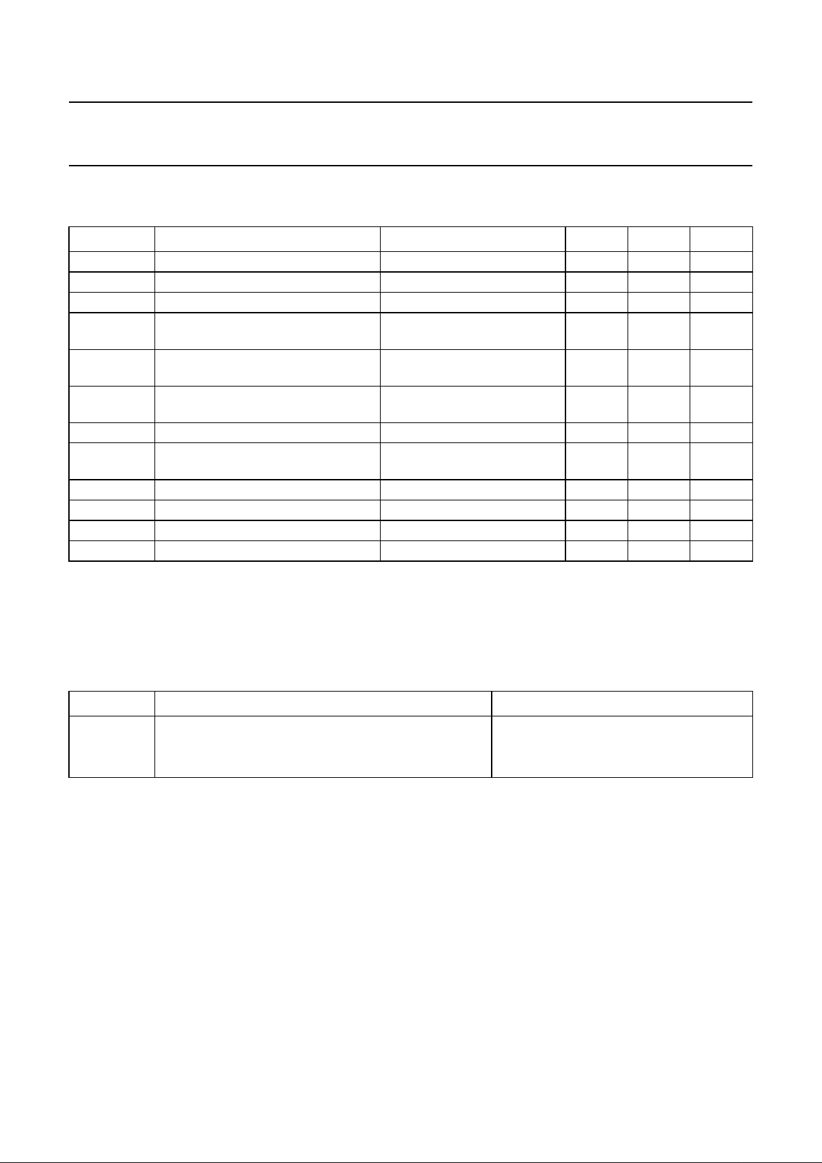
QUICK REFERENCE DATA
ORDERING INFORMATION
SYMBOL PARAMETER CONDITIONS MIN. TYP. MAX. UNIT
V
CCA
analog supply voltage 4.75 5.0 5.25 V
V
CCD
digital supply voltage 4.75 5.0 5.25 V
V
CCO
output supply voltage 4.75 5.0 5.25 V
I
CCA
analog supply current − 95 100 mA
I
CCD
digital supply current − 40 45 mA
I
CCO
output supply current − 35 40 mA
ILE DC integral linearity error f
clk
= 4 MHz −±1.0 ±2.0 LSB
DLE DC differential linearity error f
clk
= 4 MHz −±0.6 ±1.0 LSB
AILE AC integral linearity error f
clk
= 40 MHz;
fi= 4.43 MHz
−±1.2 ±2.0 LSB
f
clk(max)
maximum clock frequency
TDA8760K/2 20 −−MHz
TDA8760K/4 40 −−MHz
P
tot
total power dissipation − 850 970 mW
T
amb
operating ambient temperature 0 − +70 °C
TYPE
NUMBER
PACKAGE SAMPLING
FREQUENCY
(MHz)
NAME DESCRIPTION VERSION
TDA8760K/2
PLCC44 plastic leaded chip carrier; 44 leads SOT187-2
20
TDA8760K/4 40
1996 Sep 12 4
Philips Semiconductors Product specification
10-bit high-speed analog-to-digital
converter
TDA8760
This text is here in white to force landscape pages to be rotated correctly when browsing through the pdf in the Acrobat reader.This text is here in
_white to force landscape pages to be rotated correctly when browsing through the pdf in the Acrobat reader.This text is here inThis text is here in
white to force landscape pages to be rotated correctly when browsing through the pdf in the Acrobat reader. white to force landscape pages to be ...
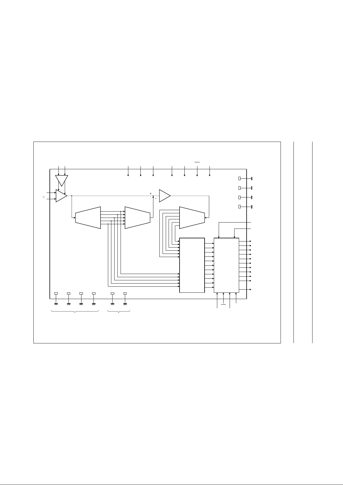
BLOCK DIAGRAM
handbook, full pagewidth
MBD222 - 2
TTL
OUTPUTS
27
D9 (MSB)
29
D8
31
D7
32
D6
33
D5
34
D4
35
D3
36
D2
40
D1
41
D0 (LSB)
26
IR
data outputs
43
V
CCO4
42
V
CCO3
25
V
CCO1
28
CCO2
2322
CS
OTC
V
ERROR
CORECTION
FINE
ADC
FINE
DAC
COARSE
ADC
AMP
SAMPLE
AND
HOLD
10
11
AMP
V
refHVrefL
15 14
V
I
V
I
CCD1
V
3
CCD2
V
21
CLK2CLK
1
CCA3
V
17
CCA2
V
13
CCA1
V
7
24
OGND1
output ground
30
OGND2
output ground
37
OGND3
output ground
44
OGND4
output ground
TDA8760
8
AGND19AGND212AGND316AGND44DGND120DGND2
digital groundanalog ground
Fig.1 Block diagram for SO187 package.
1996 Sep 12 5
Philips Semiconductors Product specification
10-bit high-speed analog-to-digital
converter
TDA8760
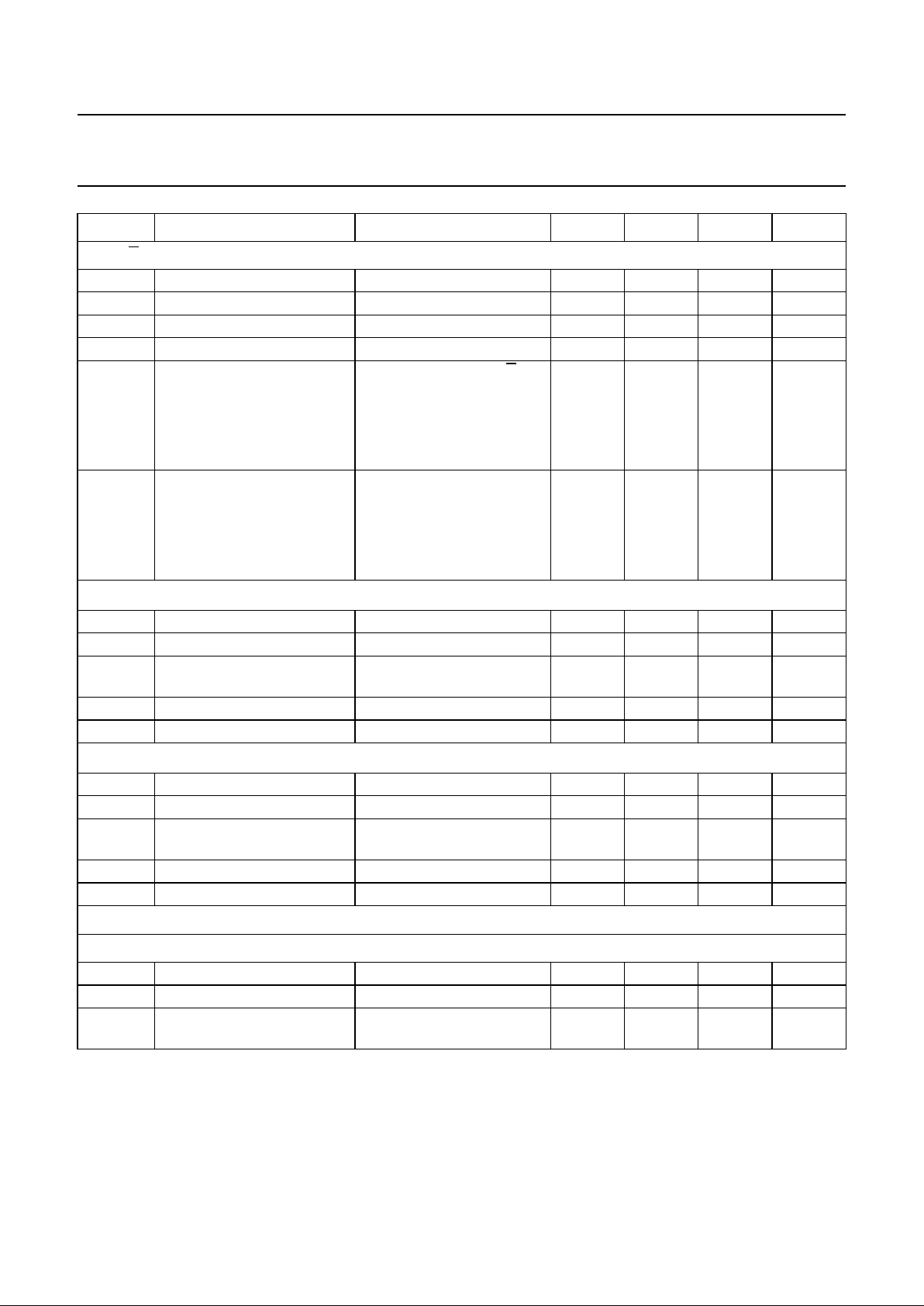
PINNING
SYMBOL PIN DESCRIPTION
CLK 1 clock input
CLK 2 complementary clock input
V
CCD1
3 digital supply voltage (+5 V)
DGND1 4 digital ground
n.c. 5 not connected
n.c. 6 not connected
V
CCA1
7 analog supply voltage (+5 V)
AGND1 8 analog ground
AGND2 9 analog ground
V
I
10 analog input voltage
V
I
11 complementary analog input voltage
AGND3 12 analog ground
V
CCA2
13 analog supply voltage (+5 V)
V
refL
14 reference voltage LOW
V
refH
15 reference voltage HIGH
AGND4 16 analog ground
V
CCA3
17 analog supply voltage (+5 V)
n.c. 18 not connected
n.c. 19 not connected
DGND2 20 digital ground
V
CCD2
21 digital supply voltage (+5 V)
CS 22 chip select input (TTL level input; active HIGH)
OTC 23 output two’s complement
OGND1 24 output ground
V
CCO1
25 output supply voltage (+5 V)
IR 26 in-range output
D9 27 data output, bit 9 (MSB)
V
CCO2
28 output supply voltage (+5 V)
D8 29 data output, bit 8
OGND2 30 output ground
D7 31 data output, bit 7
D6 32 data output, bit 6
D5 33 data output, bit 5
D4 34 data output, bit 4
D3 35 data output, bit 3
D2 36 data output, bit 2
OGND3 37 output ground
n.c. 38 not connected
n.c. 39 not connected
D1 40 data output, bit 1
1996 Sep 12 6
Philips Semiconductors Product specification
10-bit high-speed analog-to-digital
converter
TDA8760
D0 41 data output, bit 0 (LSB)
V
CCO3
42 output supply voltage (+5 V)
V
CCO4
43 output supply voltage (+5 V)
OGND4 44 output ground
SYMBOL PIN DESCRIPTION
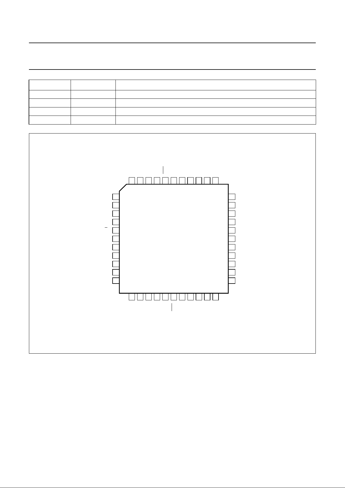
Fig.2 Pin configuration for SOT187-2.
handbook, full pagewidth
MGA928-1
7
8
9
10
11
12
13
14
15
16
17
39
38
37
36
35
34
33
32
31
30
29
18
19
20
21
22
23
24
25
26
27
28
6
5
4
3
2
1
44
43
42
41
40
OGND2
D2
D3
D4
D5
D6
D7
D8
OGND3
TDA8760
refH
V
refL
V
V
I
AGND2
V
CCA1
V
I
V
CCA2
V
CCA3
AGND4
AGND3
AGND1
n.c.
n.c.
V
CCO4
D0 (LSB)
D1
DGND1
CLK
V
CCD1
CLK
n.c.
n.c.
V
CCO3
OGND4
V
CCO2
D9 (MSB)
IR
V
CCO1
OTC
CS
DGND2
V
CCD2
n.c.
n.c.
OGND1
1996 Sep 12 7
Philips Semiconductors Product specification
10-bit high-speed analog-to-digital
converter
TDA8760
LIMITING VALUES
In accordance with the Absolute Maximum Rating System (IEC 134).
HANDLING
Inputs and outputs are protected against electrostatic discharges in normal handling. However, to be totally safe, it is
desirable to take normal precautions appropriate to handling integrated circuits.
THERMAL CHARACTERISTICS
SYMBOL PARAMETER CONDITIONS MIN. MAX. UNIT
V
CCA
analog supply voltage −0.3 +7.0 V
V
CCD
digital supply voltage −0.3 +7.0 V
V
CCO
output supply voltage −0.3 +7.0 V
∆V
CC1
supply voltage difference between
V
CCA
and V
CCD
−0.5 +0.5 V
∆V
CC2
supply voltage difference between
V
CCO
and V
CCD
−0.5 +0.5 V
∆V
CC3
supply voltage difference between
V
CCA
and V
CCO
−0.5 0.5 V
V
I
input voltage referenced to AGND 0.3 V
CCA
V
V
I(p-p)
input voltage for differential clock
drive (peak-to-peak value)
− V
CCD
V
I
O
output current − 10 mA
T
stg
storage temperature −55 +150 °C
T
amb
operating ambient temperature 0 +70 °C
T
j
junction temperature − +150 °C
SYMBOL PARAMETER THERMAL RESISTANCE
R
th j-a
Thermal resistance from junction to ambient in free air
TDA8760K/4 35 K/W
TDA8760K/2 46 K/W
1996 Sep 12 8
Philips Semiconductors Product specification
10-bit high-speed analog-to-digital
converter
TDA8760
CHARACTERISTICS
V
CCA=VCCD=VCCO
= 4.75 to 5.25 V; AGND and DGND shorted together;
V
CCA
− V
CCD=VCCO
− V
CCD=VCCA
− V
CCO
= −0.25 to +0.25 V; T
amb
=0to+70°C; unless otherwise specified.
Typical values measured at V
CCA=VCCD=VCCO
=5V; T
amb
=25°C.
SYMBOL PARAMETER CONDITIONS MIN. TYP. MAX. UNIT
Supplies
V
CCA
analog supply voltage 4.75 5.0 5.25 V
V
CCD
digital supply voltage 4.75 5.0 5.25 V
V
CCO
output supply voltage 4.75 5.0 5.25 V
I
CCA
analog supply current − 95 100 mA
I
CCD
digital supply current − 40 45 mA
I
CCO
output supply current all outputs LOW − 35 40 mA
Inputs
CLK
AND CLK (REFERENCED TO DGND); note 1
V
IL
LOW level input voltage 0 − 0.8 V
V
IH
HIGH level input voltage 2.0 − V
CCD
V
I
IL
LOW level input current V
clk
or V
clk
= 0.4 V −400 −−mA
I
IH
HIGH level input current V
clk
or V
clk
= 2.0 V −−100 mA
V
clk
or V
clk=VCCD
−−300 mA
Z
I
input impedance f
clk
= 40 MHz − 2 − kΩ
C
I
input capacitance f
clk
= 40 MHz − 4.5 − pF
∆V
clk
AC input voltage for
switching (V
clk
− V
clk
)
DC level = 1.5 V 0.5 − 2.0 V
DC level = 2.5 V 1.5 − 5.0 V
OTC AND CS (REFERENCED TO DGND); see Table 3
V
IL
LOW level input voltage 0 − 0.8 V
V
IH
HIGH level input voltage 2.0 − V
CCD
V
I
IL
LOW level input current VIL= 0.8 V −400 −−µA
I
IH
HIGH level input current VIH= 2.0 V −−20 µA
1996 Sep 12 9
Philips Semiconductors Product specification
10-bit high-speed analog-to-digital
converter
TDA8760
V
I
AND V
I
(REFERENCED TO AGND); see also Tables 1 and 2
I
IL
LOW level input current V
refH
− V
refL
= 1.5 V − 7 −µA
I
IH
HIGH level input current V
refH
− V
refL
= 1.5 V − 22 −µA
Z
I
input impedance fi= 4.43 MHz − 2 − kΩ
C
I
input capacitance fi= 4.43 MHz − 4.5 − pF
V
Ioffset(d)
input offset voltage differential mode; VI= VI;
output code 511; Table 1
V
CCA
= 5 V 3.3 3.4 3.6 V
V
CCA
= 4.75 V 3.2 − 3.45 V
V
CCA
= 5.25 V 3.3 − 3.8 V
V
Ioffset(s)
input offset voltage single mode; VI=V
Ioffset(s)
;
output code 511; Table 2
V
CCA
= 5 V 3.6 3.7 3.8 V
V
CCA
= 4.75 V 3.5 − 3.65 V
V
CCA
= 5.25 V 3.6 − 4.0 V
Voltage controlled regulator inputs V
refH
and V
refL
(referenced to AGND); differential input
V
refH
reference voltage HIGH 4.0 4.5 V
CCA
V
V
refL
reference voltage LOW 2.5 3.0 3.5 V
V
I(p-p)
input voltage amplitude
(peak-to-peak value)
1.4 1.5 1.6 V
I
refH
input current at V
refH
− 10 −µA
I
refL
input current at V
refL
− 10 −µA
Voltage controlled regulator inputs V
refH
and V
refL
(referenced to AGND); single input
V
refH
reference voltage HIGH 4.0 4.4 V
CCA
V
V
refL
reference voltage LOW 2.5 3.0 3.5 V
V
I(p-p)
input voltage amplitude
(peak-to-peak value)
1.3 1.4 1.5 V
I
refH
input current at V
refH
− 10 −µA
I
refL
input current at V
refL
− 10 −µA
Outputs (referenced to DGND)
D
IGITAL OUTPUTS D9 TO D0 AND IR (REFERENCED TO DGND)
V
OL
LOW level output voltage IO= 2 mA 0 − 0.4 V
V
OH
HIGH level output voltage IO= −0.4 mA 2.4 − V
CCD
V
I
O
output current in 3-state
mode
0.4V<VO<V
CCO
−20 − +20 µA
SYMBOL PARAMETER CONDITIONS MIN. TYP. MAX. UNIT
 Loading...