

Philips TDA8758G-C1 Datasheet
DATA SH EET
Product specification
Supersedes data of 1995 Mar 22
File under Integrated Circuits, IC02
1996 Feb 01
INTEGRATED CIRCUITS
TDA8758
YC 8-bit low-power
analog-to-digital video interface
1996 Feb 01 2
Philips Semiconductors Product specification
YC 8-bit low-power analog-to-digital
video interface
TDA8758
FEATURES
• Two 8-bit ADCs:
– one Luminance or CVBS channel
– one Chrominance channel
• Sampling rate up to 32 MHz
• Binary or two's complement 3-state TTL outputs for
each channel
• Internal reference voltage regulator
• TTL-compatible digital inputs and outputs
• Power dissipation of 530 mW (typical)
• Input selector circuit (five selectable video inputs for
CVBS or YC processing)
• Peak white enable input
• Clamp and Automatic Gain Control (AGC) functions for
Y/CVBS channel (clamping on code 64 and Peak White
level control at code 255)
• Clamp function for C channel (code 128)
• No sample-and-hold circuit required.
APPLICATIONS
• Video signal decoding
• Digital picture processing
• Frame grabbing
• Multimedia with the Philips Desktop Video chip set (and
especially SAA7196 multistandard decoder and scaler).
GENERAL DESCRIPTION
The TDA8758 is an 8-bit video high-speed low-power
analog-to-digital conversion (ADC) interface for YC and
CVBS signal processing. It converts 1-of-3 CVBS input
signals or 1-of-2 YC input signals into binary or two’s
complement words at a sampling rate of 32 MHz.
All analog signal inputs are digitally clamped and an ADC
interface is provided on the Y/CVBS channel. A fast
precharge on clamp and AGC is provided for start-up.
All digital inputs and outputs are TTL compatible.
QUICK REFERENCE DATA
ORDERING INFORMATION
SYMBOL PARAMETER CONDITIONS MIN. TYP. MAX. UNIT
V
CCA
analog supply voltage 4.75 5.0 5.25 V
V
CCD
digital supply voltage 4.75 5.0 5.25 V
V
CCO
output stages supply voltage 4.75 5.0 5.25 V
I
CCA
analog supply current − 59 70 mA
I
CCD
digital supply current − 28 40 mA
I
CCO
output supply current CL=15pF − 19 28 mA
ILE DC integral linearity error −±0.75 ±1.5 LSB
DLE DC differential linearity error −±0.4 ±1.0 LSB
EB effective bits
(from video input to digital outputs)
f
clk
= 32 MHz;
fi= 4.43 MHz
− 7.1 − bits
f
clk(max)
maximum clock frequency 30 32 − MHz
B maximum −3 dB bandwidth
(input preamplifier)
full-scale; 0 dB gain − 15 − MHz
α
ct
crosstalk between Y and C channels
and each video input
−−63 −55 dB
P
tot
total power dissipation − 530 724 mW
TYPE
NUMBER
PACKAGE
NAME DESCRIPTION VERSION
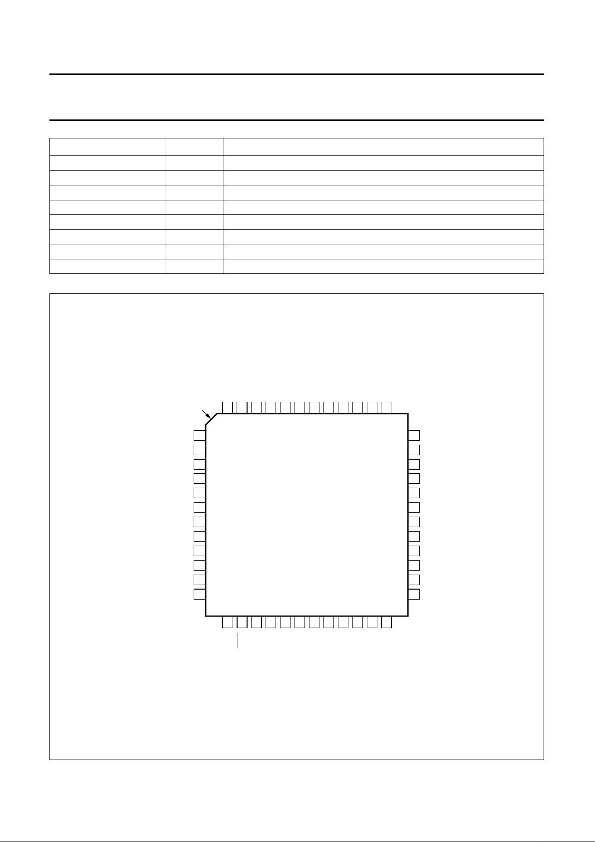
TDA8758G LQFP48 plastic low profile quad flat package; 48 leads; body 7 × 7 × 1.4 mm SOT313-2
1996 Feb 01 3
Philips Semiconductors Product specification
YC 8-bit low-power analog-to-digital video
interface
TDA8758
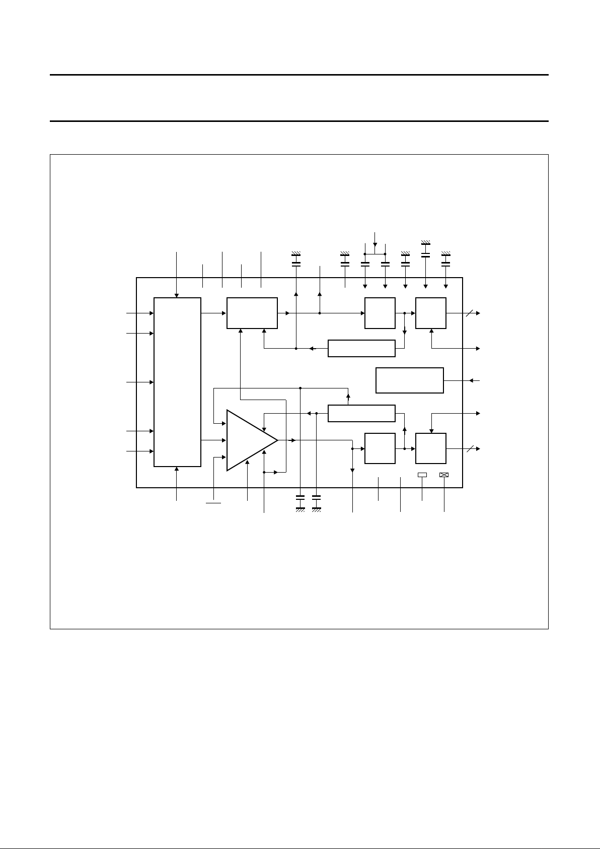
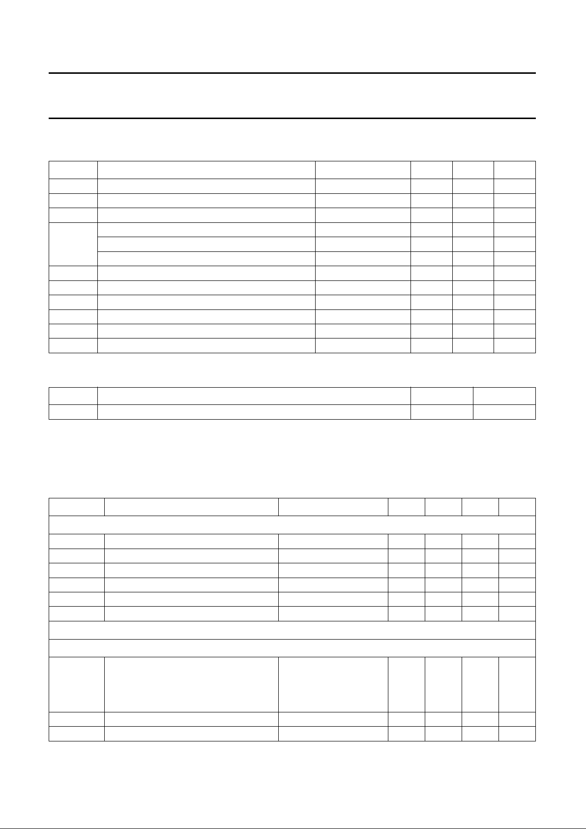
BLOCK DIAGRAM
Fig.1 Block diagram.
handbook, full pagewidth
MGB469 - 1
TDA8758
CLAMP
LEVEL 128
ADC
INPUT
SELECTOR
COMPARATOR
TTL
TIMING
GENERATOR
COMPARATORS
48 45 8 44 17 1 46 15
ADC TTL
713
AGC &
CLAMP 64
1614 19 20
2
4
6
9
11
5
10 21 41 32
33
to
40
47
42
22
23
to
30
12 31 43 18 3
8
8
C7 to C0
Y7 to Y0
OGND2
OFC
DEC2
ANOUTC
REG1
CCA
V
OGND1
CLK
DEC1
CHROM2
AGND
CHROM1
SEL2
CVBS3
SDN
Y2/CVBS2
Y1/CVBS1
SEL1
PWE
DEC3
ANOUTY
REG2
DGND
GATE A
GATE B
OFY
V
CCO2
C
CLPC
V
CCO1
C
CLPY
V
CCA
C
AGC
V
CCD
1996 Feb 01 4
Philips Semiconductors Product specification
YC 8-bit low-power analog-to-digital video
interface
TDA8758
PINNING
SYMBOL PIN DESCRIPTION
DEC1 1 decoupling input 1
CHROM2 2 chrominance analog voltage input 2
AGND 3 analog ground
CHROM1 4 chrominance analog voltage input 1
SEL2 5 selection control input 2
CVBS3 6 luminance analog voltage input 3
C
CLPY
7 Y channel clamping capacitor
SDN 8 stabilizer decoupling node
Y2/CVBS2 9 luminance analog voltage input 2
V
CCA
10 analog supply voltage (+5 V)
Y1/CVBS1 11 luminance analog voltage input 1
SEL1 12 selection control input 1
C
AGC
13 AGC capacitor
PWE 14 peak white enable input (active LOW)
DEC3 15 decoupling input 3
ANOUTY 16 analog output for Y channel
REG2 17 decoupling input 2 (internal stabilization loop decoupling)
DGND 18 digital ground
GATE A 19 AGC control input
GATE B 20 clamp control input
V
CCD
21 digital supply voltage (+5 V)
OFY 22 Y channel output format/chip enable (3-state input)
Y7 23 Y channel data output; bit 7 (MSB)
Y6 24 Y channel data output; bit 6
Y5 25 Y channel data output; bit 5
Y4 26 Y channel data output; bit 4
Y3 27 Y channel data output; bit 3
Y2 28 Y channel data output; bit 2
Y1 29 Y channel data output; bit 1
Y0 30 Y channel data output; bit 0 (LSB)
OGND2 31 output ground 2
V
CCO2
32 output supply voltage 2 (+5 V)
C7 33 C channel data output; bit 7 (MSB)
C6 34 C channel data output; bit 6
C5 35 C channel data output; bit 5
C4 36 C channel data output; bit 4
C3 37 C channel data output; bit 3
C2 38 C channel data output; bit 2
C1 39 C channel data output; bit 1
C0 40 C channel data output; bit 0 (LSB)
1996 Feb 01 5
Philips Semiconductors Product specification
YC 8-bit low-power analog-to-digital video
interface
TDA8758
V
CCO1
41 output supply voltage 1 (+5 V)
CLK 42 clock input
OGND1 43 output ground 1
REG1 44 decoupling input 1 (internal stabilization loop decoupling)
ANOUTC 45 analog output for C channel
DEC2 46 decoupling input 2
OFC 47 C channel output format/chip enable (3-state input)
C
CLPC
48 C channel clamping capacitor
SYMBOL PIN DESCRIPTION
Fig.2 Pin configuration.
handbook, full pagewidth
1
2
3
4
5
6
7
8
9
10
11
36
35
34
33
32
31
30
29
28
27
26
13
14
15
16
17
18
19
20
21
22
23
48
47
46
45
44
43
42
41
40
39
38
12
24 37
25
pin 1
index
corner
TDA8758
MGB470
C4
C5
C6
C7
OGND2
Y0
Y1
Y2
Y3
Y4
Y5
DEC1
CHROM2
AGND
CHROM1
SEL2
CVBS3
SDN
Y2/CVBS2
Y1/CVBS1
SEL1
V
CCO2
OFC
DEC2
ANOUTC
REG1
OGND1
CLK
C0C1C2
C3
C
CLPC
V
CCO1
C
CLPY
V
CCA
PWE
DEC3
ANOUTY
REG2
DGND
GATE A
GATE B
OFY
Y7
Y6
C
AGC
V
CCD

1996 Feb 01 6
Philips Semiconductors Product specification
YC 8-bit low-power analog-to-digital video
interface
TDA8758
FUNCTIONAL DESCRIPTION
The TDA8758 provides a simple interface between CVBS
or Y/C analog signals and a digital colour decoder.
Video inputs selection
The input selector allows a choice from different video
sources, and has one of the following configurations:
A: Two Y/C and one CVBS signals
B: One Y/C and two CVBS signals
C: Three CVBS signals (only the Y channel is used).
The wiring of the five video inputs (pins 2, 4, 6, 9 and 11)
and the control of the two selection inputs (pins 5 and 12)
will depend on the available video sources.
• In configuration A, connect as follows:
– Y1 to pin 11
– C1 to pin 4
– Y2 to pin 9
– C2 to pin 2
– CVBS3 to pin 6.
Keep SEL2 (pin 5) LOW and select Y1/C1 or Y2/C2 by
switching SEL1 (pin 12).
CVBS3 is selected with SEL1 and SEL2 HIGH.
• In configuration B, replace Y1 (or Y2) by a CVBS input
(no more C1 or C2). The selection mode is the same.
• In configuration C, connect as follows:
– CVBS1 to pin 11
– CVBS2 to pin 9
– CVBS3 to pin 6.
Use both SEL1 and SEL2 to select inputs.
Remark: the video inputs selection is a static selection.
Synchronization pulses
GATE A and GATE B pulses are synchronization pulses
occurring during the sync period and rear porch
respectively. They should be distinct.
On the Y channel, the digital output of the ADC is
compared to internal digital reference levels. The resultant
outputs control the charge or discharge current of a
capacitor connected to the C
AGC
pin. The voltage across
this capacitor controls the gain of the video amplifier.
This is the control loop.
The sync level comparator is active during a positive-going
pulse at the GATE A input. This means that sync pulse of
the composite video signal is used as an amplitude
reference. The bottom of the sync pulse is adjusted to
obtain a digital output of logic 1 at the converter Y output.
As the black level is digital level 64, the sync pulse will
have a digital amplitude of 64 LSBs.
The Peak White control loop is active when the selection
pin
PWE is LOW. Then, if the Y video signal exceeds the
digital code of 255, it will be limited to avoid any over-range
of the converter.
The clamp level control is accomplished by using the same
techniques as used for the gain control. On both Y and C
channels, the black level digital comparators are active
during a positive-going pulse at the GATE B input. On the
Y channel, the clamping capacitor connected to the C
CLPY
pin will be charged or discharged to adjust the digital
output to code 64. On the C channel, the clamping
capacitor connected to the C
CLPC
pin will be charged or
discharged to adjust the digital output to code 128.
1996 Feb 01 7
Philips Semiconductors Product specification
YC 8-bit low-power analog-to-digital video
interface
TDA8758
LIMITING VALUES
In accordance with the Absolute Maximum Rating System (IEC 134).
THERMAL CHARACTERISTICS
CHARACTERISTICS
V
CCA=V10
to V3= 4.75 to 5.25 V; V
CCD=V21
to V18= 4.75 to 5.25 V; V
CCO1=V41
to V43= 4.75 to 5.25 V;
V
CC02=V32
to V31= 4.75 to 5.25 V; AGND and DGND shorted together; V
CCA
to V
CCD
= −0.25 to +0.25 V;
V
CCO
to V
CCD
= −0.25 to +0.25 V; V
CCA
to V
CCO
= −0.25 to +0.25 V; T
amb
= 0 to +70 °C; typical values measured
at V
CCA=VCCD=VCCO
= 5 V and T
amb
=25°C; unless otherwise specified.
SYMBOL PARAMETER CONDITIONS MIN. MAX. UNIT
V
CCA
analog supply voltage −0.3 +7.0 V
V
CCD
digital supply voltage −0.3 +7.0 V
V
CCO
output supply voltage −0.3 +7.0 V
∆V
CC
supply voltage difference between V
CCA
and V
CCD
−1.0 +1.0 V
supply voltage difference between V
CCO
and V
CCD
−1.0 +1.0 V
supply voltage difference between V
CCA
and V
CCO
−1.0 +1.0 V
V
I
input voltage referenced to AGND − 5.0 V
V
clk(p-p)
AC input voltage for switching (peak-to-peak value) referenced to DGND − V
CCO
V
I
O
output current − +6 mA
T
stg
storage temperature −55 +150 °C
T
amb
operating ambient temperature 0 +70 °C
T
j
junction temperature − +150 °C
SYMBOL PARAMETER VALUE UNIT
R
th j-a
thermal resistance from junction to ambient in free air 72 K/W
SYMBOL PARAMETER CONDITIONS MIN. TYP. MAX. UNIT
Supplies
V
CCA
analog supply voltage 4.75 5.0 5.25 V
V
CCD
digital supply voltage 4.75 5.0 5.25 V
V
CCO
output stages supply voltage 4.75 5.0 5.25 V
I
CCA
analog supply current − 59 70 mA
I
CCD
digital supply current − 28 40 mA
I
CCOtot
total output supply current CL=15pF − 19 28 mA
Video amplifier inputs
Y1/CVBS1, Y2/CVBS2, CVBS3, CHROM1
AND CHROM2 INPUTS
V
I(p-p)
input voltage (peak-to-peak value) AGC load with external
capacitor; note 1
Y channel 0.7 − 1.4 V
C channel − 1.0 − V
|Z
i
| input impedance fi= 6 MHz − 25 − kΩ
C
I
input capacitance fi= 6 MHz − 2 − pF
1996 Feb 01 8
Philips Semiconductors Product specification
YC 8-bit low-power analog-to-digital video
interface
TDA8758
SEL1 AND SEL2 TTL INPUTS; see Table 1
V
IL
LOW level input voltage 0 − 0.8 V
V
IH
HIGH level input voltage 2.0 − V
CCD
V
I
IL
LOW level input current VI= 0.4 V −400 −−µA
I
IH
HIGH level input current VI= 2.7 V −−20 µA
GATE A AND GATE B TTL INPUTS; see Figs 5 and 6
V
IL
LOW level input voltage 0 − 0.8 V
V
IH
HIGH level input voltage 2.0 − V
CCD
V
I
IL
LOW level input current VI = 0.4 V −400 −−µA
I
IH
HIGH level input current VI = 2.7 V −−20 µA
AGC INPUT (PIN 13); see Fig.8
V
13(min)
AGC voltage for minimum gain at −3dB − 3.3 − V
V
13(max)
AGC voltage for maximum gain at +3 dB − 3.75 − V
I
12
AGC output current see Table 2
C-CHANNEL CLAMP INPUT (PIN 48)
V
48
CLAMP voltage for code 128 output − 3.45 − V
I
48
CLAMP output current see Table 3
Y-CHANNEL CLAMP INPUT (PIN 7)
V
7
CLAMP voltage for code 64 output − 3.70 − V
I
7
CLAMP output current see Table 3
Video amplifier dynamic characteristics
α
ct
crosstalk between video inputs
(pins 2, 4, 6, 9 and 11)
V
CCA
= 4.75 to 5.25 V −−63 −55 dB
B −3 dB bandwidth − 15 − MHz
∆G gain range −3 − +3 dB
G
stab
gain stability as a function of:
supply voltage f
i
= 4.43 MHz −−0.5 %
supply voltage and temperature −−6%
Analog-to-digital converter inputs
CLK
INPUT (PIN 42)
V
IL
LOW level input voltage 0 − 0.8 V
V
IH
HIGH level input voltage 2.0 − V
CCD
V
I
IL
LOW level input current V
clk
= 0.4 V −400 −−µA
I
IH
HIGH level input current V
clk
= 2.7 V −−20 µA
C
I
input capacitance f
clk
= 32 MHz − 2 − pF
SYMBOL PARAMETER CONDITIONS MIN. TYP. MAX. UNIT
 Loading...