

Philips tda8755 DATASHEETS
INTEGRATED CIRCUITS
DATA SH EET
TDA8755
YUV 8-bit video low-power
analog-to-digital interface
Product specification
Supersedes data of June 1994
File under Integrated Circuits, IC02
Philips Semiconductors
1995 Mar 09
Philips Semiconductors Product specification
YUV 8-bit video low-power
analog-to-digital interface
FEATURES
• 8-bit resolution
• Sampling rate up to 20 MHz
• TTL compatible digital inputs
• 3-state TTL outputs
• U, V two's complement outputs
• Y binary output
• Power dissipation of 550 mW (typical)
• Low analog input capacitance, no buffer amplifier
required
• High signal-to-noise ratio over a large analog input
frequency range
• Track-and-hold included
• Clamp functions included
• UV multiplexed ADC
• 4:1:1 output data encoder
• Stable voltage regulator included.
TDA8755
APPLICATIONS
• High speed analog-to-digital conversion for video signal
digitizing
• 100 Hz improved definition TV (IDTV).
GENERAL DESCRIPTION
The TDA8755 is a bipolar 8-bit video low-power
analog-to-digital conversion (ADC) interface for YUV
signals. The device converts the YUV analog input signal
into 8-bit coded digital words in a 4 : 1 : 1 format at a
sampling rate of 20 MHz. The U/V signals are converted in
a multiplexed manner. All analog signal inputs are digitally
clamped and a fast precharge is provided for start-up.
All digital inputs and outputs are TTL compatible. Frame
synchronization is supported in a multiplexed manner.
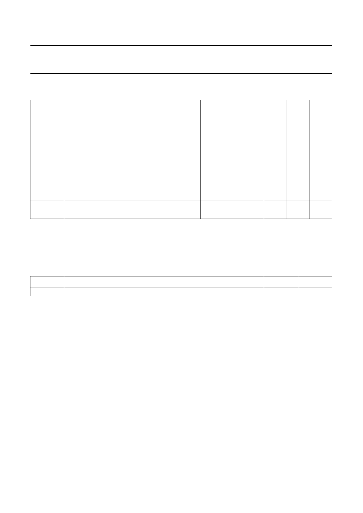
QUICK REFERENCE DATA
SYMBOL PARAMETER CONDITIONS MIN. TYP. MAX. UNIT
V
CCA
V
CCD
V
CCO
I
CCA
I
CCD
I
CCO
INL DC integral non-linearity f
DNL DC differential non-linearity f
analog supply voltage 4.75 5.0 5.25 V
digital supply voltage 4.75 5.0 5.25 V
output stages supply voltage 4.75 5.0 5.25 V
analog supply current − 46 55 mA
digital supply current − 55 66 mA
output stages supply current − 912mA
= 2 MHz −±0.4 ±1 LSB
clk
= 2 MHz −±0.3 ±0.5 LSB
clk
EB effective bits − 7.1 − bits
f
clk(max)
P
tot
maximum clock frequency 20 −−MHz
total power dissipation − 550 700 mW
ORDERING INFORMATION
PACKAGE
TYPE NUMBER
PINS PIN POSITION MATERIAL CODE
TDA8755T 32 SO32L plastic SOT287-1
1995 Mar 09 2
Philips Semiconductors Product specification
YUV 8-bit video low-power
analog-to-digital interface
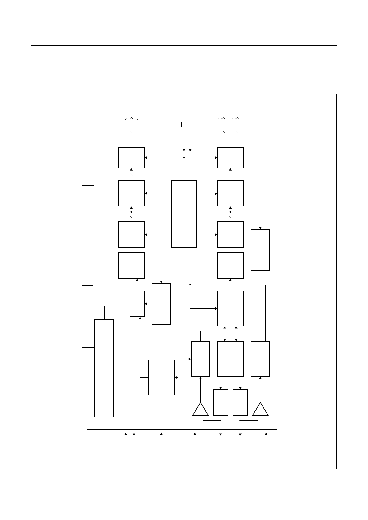
BLOCK DIAGRAM
2413
REG1 REG2 REG3
Y
D0
D7
8
24
31
TTL
I / O
8
8-BIT
PIPELINE
8
ADC
8-BIT
CLK
CE
HREF
17
14
16
TIMING GENERATOR
V
D'0
D'1
2
192021
TTL
U AND V
8
8-BIT
U
D'2
D'3
2
22
I / O
DATA
ENCODER
ADC
TDA8755
MLA734 - 1
TDA8755
CCO AGND DGND SDN n.c.
V
CCD
V
6 322310188 1
CCA
V
AND
HOLD
TRACK
Y
CLAMP
VOLTAGE REGULATOR
SUPPLY AND REFERENCE
5
3
16
COMPARATOR
LOGIC
CLAMP
15
TRACK
7
AND
HOLD
AND
HOLD
TRACK
ANALOG
MULTIPLEXER
DIGITAL
MULTIPLEXER
CLAMPUCLAMP
11
V
12
128
COMPARATOR
AND
HOLD
TRACK
9
handbook, full pagewidth
Fig.1 Block diagram.
INY
CLPY
CLP
1995 Mar 09 3
INU
CLPU
CLPV
INV
Philips Semiconductors Product specification
YUV 8-bit video low-power
analog-to-digital interface
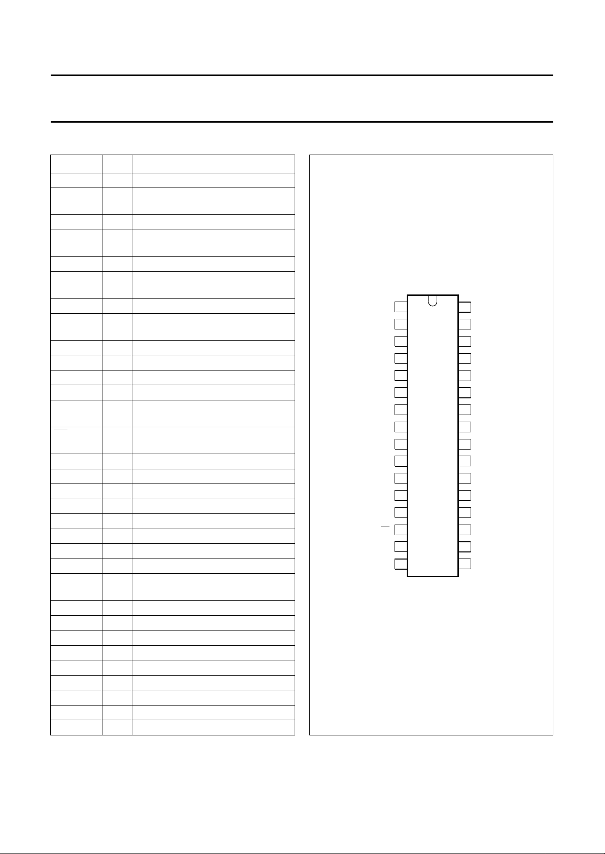
PINNING
SYMBOL PIN DESCRIPTION
n.c. 1 not connected
REG1 2 decoupling input (internal
stabilization loop decoupling)
INY 3 Y analog voltage input
REG2 4 decoupling input (internal
stabilization loop decoupling)
CLPY 5 Y clamp capacitor connection
V
CCA
INU 7 U analog voltage input
SDN 8 stabilizer decoupling node and
INV 9 V analog voltage input
AGND 10 analog ground
CLPU 11 U clamp capacitor connection
CLPV 12 V clamp capacitor connection
REG3 13 decoupling input (internal
CE 14 chip enable input (TTL level input
CLP 15 clamp control input
HREF 16 horizontal reference signal
CLK 17 clock input
DGND 18 digital ground
D'0 19 V data output; bit 0 (n−1)
D'1 20 V data output; bit 1 (n)
D'2 21 U data output; bit 0 (n−1)
D'3 22 U data output; bit 1 (n)
V
CCO
D0 24 Y data output; bit 0 (LSB)
D1 25 Y data output; bit 1
D2 26 Y data output; bit 2
D3 27 Y data output; bit 3
D4 28 Y data output; bit 4
D5 29 Y data output; bit 5
D6 30 Y data output; bit 6
D7 31 Y data output; bit 7 (MSB)
V
CCD
6 analog positive supply voltage
(+5 V)
analog reference voltage (+3.35 V)
stabilization loop decoupling)
active LOW)
23 positive supply voltage for output
stages (+5 V)
32 digital positive supply voltage (+5 V)
handbook, halfpage
1
n.c.
2
REG1
INY
3
REG2
4
5
CLPY
V
CCA
6
INU
7
SDN
8
INV
AGND
CLPU
CLPV
REG3
CE
CLP
HREF CLK
TDA8755
9
10
11
12
13
14
15
16
MLA728 - 1
V
32
31
D7
D6
30
D5
29
28
D4
D3
27
D2
26
D1
25
D0
24
V
23
D'3
22
D'2
21
D'1
20
19
D'0
18
DGND
17
Fig.2 Pin configuration.
TDA8755
CCD
CCO
1995 Mar 09 4
Philips Semiconductors Product specification
YUV 8-bit video low-power
TDA8755
analog-to-digital interface
LIMITING VALUES
In accordance with the Absolute Maximum Rating System (IEC134).
SYMBOL PARAMETER CONDITIONS MIN. MAX. UNIT
V
CCA
V
CCD
V
CCO
∆V
V
I
V
clk(p-p)
I
O
T
stg
T
amb
T
j
CC
analog supply voltage −0.3 +7.0 V
digital supply voltage −0.3 +7.0 V
output stages supply voltage −0.3 +7.0 V
supply voltage difference between V
supply voltage difference between V
supply voltage difference between V
CCA
CCO
CCA
and V
and V
and V
CCD
CCD
CCO
−1.0 +1.0 V
−1.0 +1.0 V
−1.0 +1.0 V
input voltage referenced to AGND − +5.0 V
AC input voltage for switching (peak-to-peak value) referenced to DGND − V
CCD
V
output current − +6 mA
storage temperature −55 +150 °C
operating ambient temperature 0 +70 °C
junction temperature − +150 °C
HANDLING
Inputs and outputs are protected against electrostatic discharges in normal handling. However, to be totally safe, it is
desirable to take normal precautions appropriate to handling integrated circuits.
THERMAL CHARACTERISTICS
SYMBOL PARAMETER VALUE UNIT
R
th j-a
thermal resistance from junction to ambient in free air 70 K/W
1995 Mar 09 5
Philips Semiconductors Product specification
YUV 8-bit video low-power
TDA8755
analog-to-digital interface
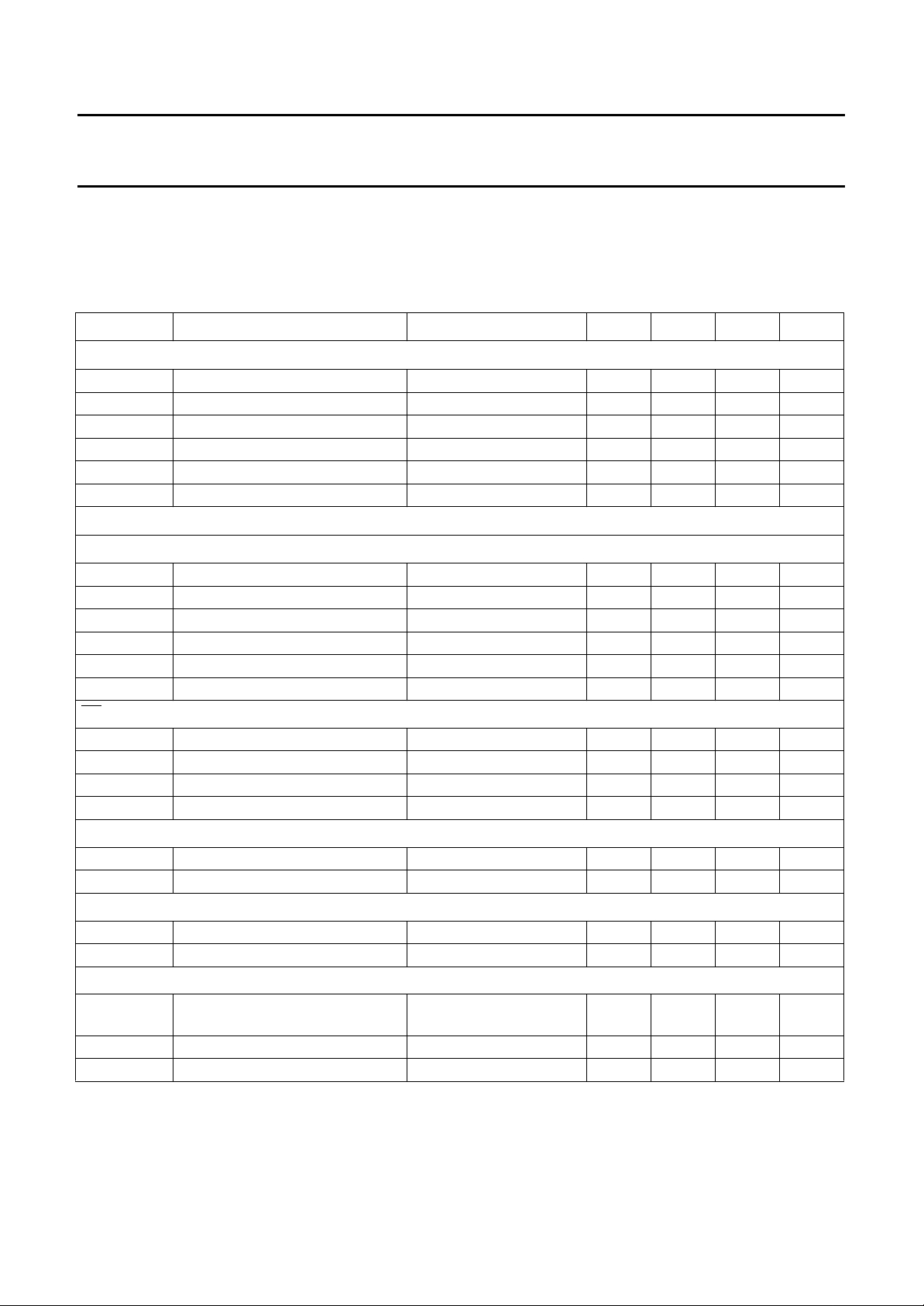
CHARACTERISTICS
V
CCA=V6
AGND and DGND shorted together; V
V
CCA
T
amb
SYMBOL PARAMETER CONDITIONS MIN. TYP. MAX. UNIT
Supply
V
CCA
V
CCD
V
CCO
I
CCA
I
CCD
I
CCO
Inputs
CLK (
V
IL
V
IH
I
IL
I
IH
Z
I
C
I
CE, CLP AND HREF (PINS 14 TO 16)
V
IL
V
IH
I
IL
I
IH
CLPY (PIN 5)
V
5
I
5
CLPU AND CLPV (PINS 11 AND 12)
V
11, 12
I
11, 12
INY (PIN 3)
V
I(p-p)
Z
I
C
I
to V10= 4.75 to 5.25 V; V
to V
= −0.25 to +0.25 V; T
CCO
CCD=V32
CCA
= 0 to +70 °C; typical values measured at V
amb
=25°C; unless otherwise specified.
analog supply voltage 4.75 5.0 5.25 V
digital supply voltage 4.75 5.0 5.25 V
output stages supply voltage 4.75 5.0 5.25 V
analog supply current − 46 55 mA
digital supply current − 55 66 mA
output stages supply current − 912mA
PIN 17)
LOW level input voltage 0 − 0.8 V
HIGH level input voltage 2.0 − V
LOW level input current V
HIGH level input current V
input impedance f
input capacitance f
LOW level input voltage 0 − 0.8 V
HIGH level input voltage 2.0 − V
LOW level input current V
HIGH level input current V
clamp voltage for 16 output code − 3.725 − V
clamp output current −±50 −µA
clamp voltage for 128 output code − 3.30 − V
clamp output current −±50 −µA
input voltage, full range
(peak-to-peak value)
input impedance fi= 6 MHz − 30 − kΩ
input capacitance fi= 6 MHz − 1 − pF
to V18= 4.75 to 5.25 V; V
to V
= −0.25 to +0.25 V; V
CCD
= 0.4 V −400 −−µA
clk
= 2.7 V −−100 µA
clk
=20MHz − 4 − kΩ
clk
=20MHz − 4.5 − pF
clk
= 0.4 V −400 −−µA
clk
= 2.7 V −−100 µA
clk
fi= 4.43 MHz 0.93 1.0 1.07 V
CCO=V23
to V
CCO
to V18= 4.75 to 5.25 V;
= −0.25 to +0.25 V;
CCD
CCA=VCCD=VCCO
= 5 V and
CCD
CCD
V
V
1995 Mar 09 6
 Loading...