

Philips TDA8754 Datasheet
INTEGRATED CIRCUITS
DATA SH EET
TDA8754
Triple high speed ADC for LCD
drive
Objective specification
File under Integrated Circuits, IC02
1998 Sep 30

Philips Semiconductors Objective specification
Triple high speed ADC for LCD drive TDA8754
FEATURES
• Triple 8-bit Analog-to-Digital Converter (ADC)
• Sampling rate up to 170 MHz
• IC controllable via a serial interface, which can be either
I2C-bus or 3-wire, selected via a TTL input pin
• IC analog input 0.5 to 1.1 V (peak-to-peak value) to
have full-scale ADC input
• Clamps for programming a clamp level through a
clamping code between −63 and +64 by steps of 1 LSB
• Controllable gain stages: gain controlled independently
on the 3 channels via the serial interface to have a
full-scale resolution to 1%
• Low gain variation at different temperatures
• Analog bandwidth of 400 MHz
• Controllable PLL via the serial interface generates the
ADC clock. It can be locked on line frequencies from
15 kHz up to 280 kHz.
• Integrated PLL divider
• Integrated clamp pulse and H and V LCD control pulses
generation (independently adjustable in position and
duration). Also a data enable signal can be generated,
independently adjustable in position and duration with
respect to HSYNC.
• The pixel clock is available at half the clock frequency
• Programmable phase clock adjustment cells
• Internal voltage regulators
• TTL compatible digital inputs
• 3.3 V CMOS compatible digital outputs
• Outputs: one port output up to 140 MHz or 2-port
demultiplexed outputs on the full speed range.
Operating mode selectable through the serial interface.
• Chip enable: high-impedance ADC output
• Power-down mode.
GENERAL DESCRIPTION
The TDA8754 is a triple 8-bit ADC with controllable gain
and clamps for the digitizing of large bandwidth
R, G, B signals. Clamp level, gain, and all the other
settings are controlled via a serial interface (either I2C-bus
or 3-wire, selected through a logic input). The gain is
optimized for stability versus temperature variations.
The IC also includes a PLL that generates the ADC clock
which can be locked to the horizontal line frequency.
The PLL jitter is minimized for high resolution PC graphics
applications. An external clock can also be used to clock
the ADC.
The clamp pulse is generated on-chip, it can be adjusted
in position (with respect to HSYNC) and duration through
the serial interface.
The horizontal and vertical control pulses for the LCD can
be adjusted in duration through the serial interface. Also a
data enable signal can be generated, independently
adjustable in position (with respect to HSYNC) and
duration through the serial interface.
Outputs: one port output up to 140 MHz or demultiplexed
2-port outputs on the full speed range. Operating mode
selectable through the serial interface.
ORDERING INFORMATION
TYPE
NUMBER
TDA8754H LQFP144 plastic low profile quad flat package; 144 leads; body 20 × 20 × 1.4 mm SOT486-1
1998 Sep 30 2
NAME DESCRIPTION VERSION
PACKAGE
Philips Semiconductors Objective specification
Triple high speed ADC for LCD drive TDA8754
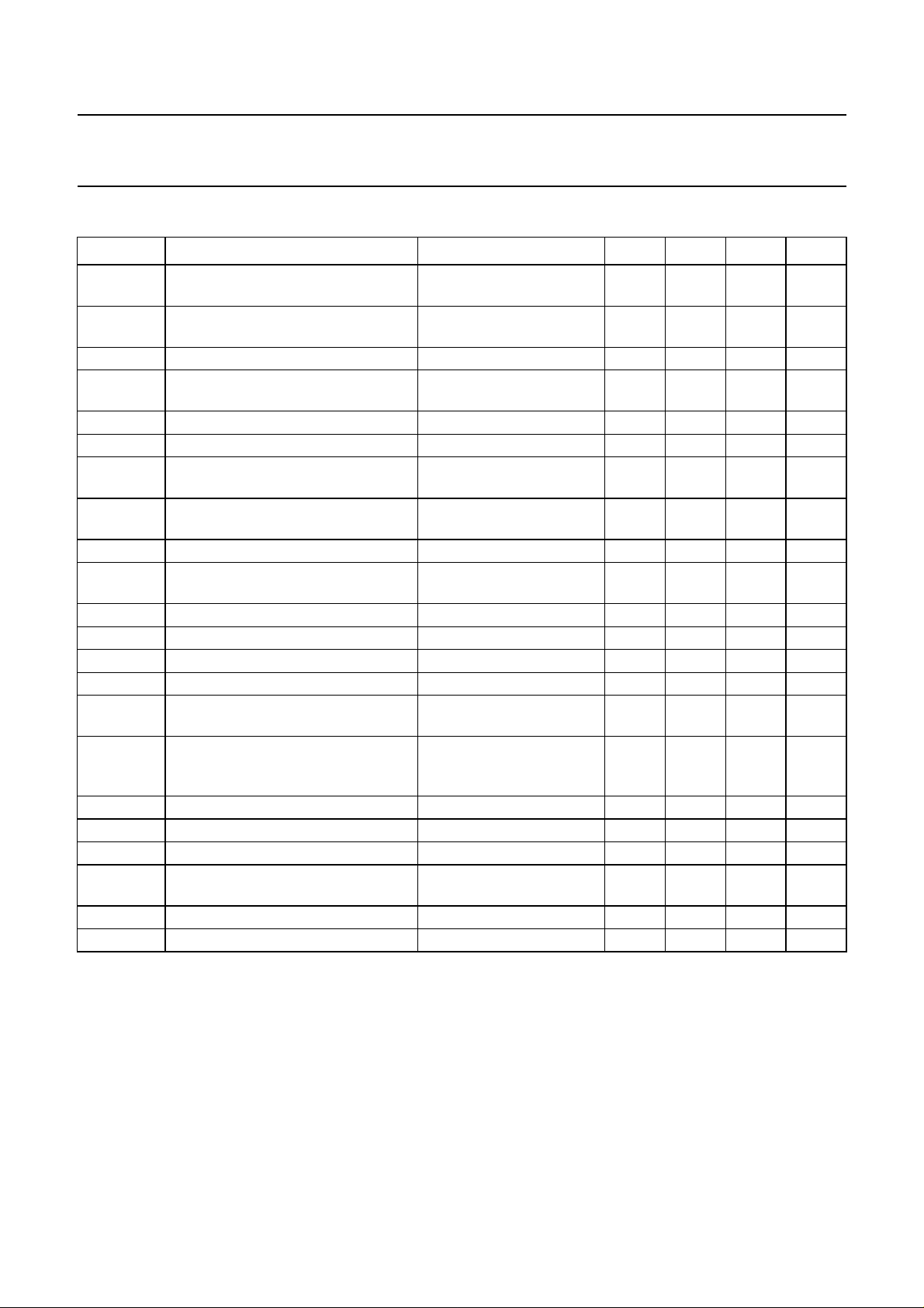
QUICK REFERENCE DATA
SYMBOL PARAMETER CONDITIONS MIN. TYP. MAX. UNIT
V
CCA
analog supply voltage for
R, G, B channels
V
DD
logic supply voltage for I2C-bus and
3-wire interface
V
CCD
V
CC(O)
digital supply voltage 4.75 5.0 5.25 V
output stages supply voltage for
R, G, B channels
V
CCA(PLL)
V
CC(O)(PLL)
I
CCA
analog PLL supply voltage 4.75 5.0 5.25 V
output PLL supply voltage 4.75 5.0 5.25 V
analog supply current for
R, G, B channels
I
DD
logic supply current for I2C-bus and
3-wire interface
I
CCD
I
CC(O)
digital supply current − tbf − mA
output stages supply current for
R, G, B channels
I
CCA(PLL)
I
CC(O)(PLL)
analog PLL supply current − tbf − mA
output PLL supply current − tbf − mA
INL DC integral non-linearity −±1±1.5 LSB
DNL DC differential non-linearity −±0.5 ±0.8 LSB
∆G
amp
gain stability versus temperature V
= 2.5 V with
ref
100 ppm/K variation
t
set
setting time of the block ADC + AGC input signal setting time
<1 ns; setting to 1%;
fi= 85 MHz
f
clk(max)
f
ref
f
PLL
j
PLL(rms)
maximum conversion rate 170 −−MHz
PLL reference clock frequency 15 − 120 kHz
output clock frequency 12 − 170 MHz
maximum PLL phase jitter
(RMS value)
D/D
P
tot
PLL
PLL divider ratio 512 − 4095
total power consumption f
= 170 MHz; ramp input − tbf 1.2 W
clk
4.75 5.0 5.25 V
3.0 5.0 5.25 V
3.0 3.3 3.6 V
− tbf − mA
− tbf − mA
− tbf − mA
−−200 ppm/K
− 2.5 3.5 ns
− 0.2 − ns
1998 Sep 30 3
 Loading...