

Philips tda8752a DATASHEETS
INTEGRATED CIRCUITS
DATA SH EET
TDA8752A
Triple high-speed Analog-to-Digital
Converter (ADC)
Product specification
Supersedes data of 1998 Dec 14
File under Integrated Circuits, IC02
1999 Feb 24

Philips Semiconductors Product specification
Triple high-speed Analog-to-Digital
Converter (ADC)
FEATURES
• Triple 8-bit ADC
• Sampling rate up to 100 MHz
• IC controllable via a serial interface, which can be either
I2C-bus or 3-wire, selected via a TTL input pin
• IC analog voltage input from 0.4 to 1.2 V (p-p) to
produce full-scale ADC input of 1 V (p-p)
• 3 clamps for programming a clamping code between
−63.5 and +64 in steps of1⁄2LSB
• 3 controllable amplifiers: gain controlled via the serial
interface to produce a full scale resolution of
peak-to-peak
• Amplifier bandwidth of 250 MHz
• Low gain variation with temperature
• PLL, controllable via the serial interface to generate the
ADC clock, which can be locked to a line frequency from
15 to 280 kHz
• Integrated PLL divider
• Programmable phase clock adjustment cells
• Internal voltage regulators
• TTL compatible digital inputs and outputs
• Chip enable high-impedance ADC output
• Power-down mode
• Possibility to use up to four ICs in the same system,
using the I2C-bus interface, or more, using the 3-wire
serial interface
• 1 W power dissipation.
1
⁄2LSB
TDA8752A
GENERAL DESCRIPTION
The TDA8752A is a triple 8-bit ADC with controllable
amplifiers and clamps for the digitizing of large bandwidth
RGB signals.
The clamp level, the gain and all of the other settings are
controlled via a serial interface (either I
serial bus, selected via a logic input).
The IC also includes a PLL that can be locked on the
horizontal line frequency and generates the ADC clock.
The PLL jitter is minimized for high resolution PC graphics
applications. An external clock can also be input to the
ADC.
It is possible to set the TDA8752A serial bus address
between four fixed values, in the event that several
TDA8752A ICs are used in a system, using the I
interface (for example, two ICs used in an odd/even
configuration).
2
C-bus or 3-wire
2
C-bus
APPLICATIONS
• R, G and B high-speed digitizing
• LCD panels drive
• LCD projection systems
• VGA and higher resolutions
• Using two ICs in parallel, higher display resolution can
be obtained; 200 MHz pixel frequency.
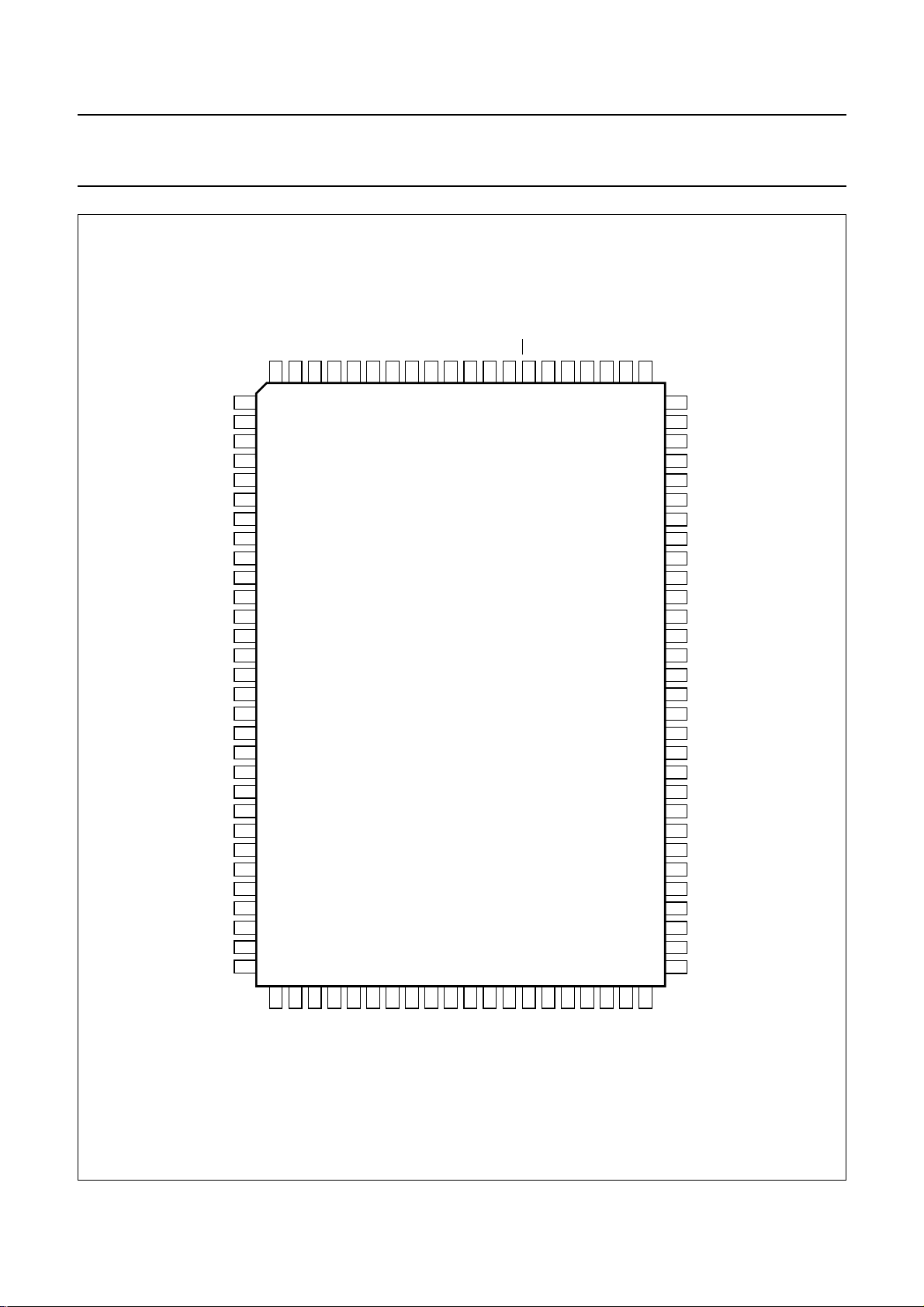
ORDERING INFORMATION
PACKAGE SAMPLING
TYPE NUMBER
TDA8752AH/6 QFP100 plastic quad flat package; 100 leads (lead length
TDA8752AH/8 100
1999 Feb 24 2
NAME DESCRIPTION VERSION
SOT317-2 60
1.95 mm); body 14 × 20 × 2.8 mm
FREQUENCY
(MHz)
Philips Semiconductors Product specification
Triple high-speed Analog-to-Digital
TDA8752A
Converter (ADC)
QUICK REFERENCE DATA
SYMBOL PARAMETER CONDITIONS MIN. TYP. MAX. UNIT
V
CCA
V
DDD
V
CCD
V
CCO
V
CCA(PLL)
V
CCO(PLL)
I
CCA
I
DDD
I
CCD
I
CCO
I
CCA(PLL)
I
CCO(PLL)
f
CLK
f
ref(PLL)
f
VCO
INL DC integral non linearity from analog input to
DNL DC differential non linearity from analog input to
∆G
amp
B amplifier bandwidth −3 dB; T
t
set
DR
PLL
P
tot
j
PLL(rms)
analog supply voltage for R, G and B channels 4.75 5.0 5.25 V
logic supply voltage for I2C-bus and 3-wire 4.75 5.0 5.25 V
digital supply voltage 4.75 5.0 5.25 V
output stages supply voltage for R, G and B channels 4.75 5.0 5.25 V
analog PLL supply voltage 4.75 5.0 5.25 V
output PLL supply voltage 4.75 5.0 5.25 V
analog supply current − 120 − mA
logic supply current for I2C-bus and 3-wire − 1.0 − mA
digital supply current − 40 − mA
output stages supply current f
= 100 MHz;
CLK
− 6 − mA
ramp input
analog PLL supply current − 28 − mA
output PLL supply current − 5 − mA
maximum clock frequency TDA8752A/6 60 −−MHz
TDA8752A/8 100 −−MHz
PLL reference clock frequency 15 − 280 kHz
VCO output clock frequency 12 − 100 MHz
−±0.5 ±1.5 LSB
digital output; full-scale;
ramp input;
f
= 100 MHz
CLK
−±0.5 ±1.0 LSB
digital output; full-scale;
ramp input;
= 100 MHz
f
CLK
/T amplifier gain stability as a function of
temperature
settling time of the ADC block plus AGC input signal settling
V
= 2.5 V with
ref
100 ppm/°C maximum
=25°C 250 −−MHz
amb
time < 1 ns; T
amb
=25°C
−−200 ppm/°C
−−6ns
PLL divider ratio 100 − 4095
total power consumption f
= 100 MHz;
CLK
− 1.0 − W
ramp input
maximum PLL phase jitter (RMS value) f
= 66.67 kHz;
ref
f
= 100 MHz
CLK
− 0.3 − ns
1999 Feb 24 3
This text is here in white to force landscape pages to be rotated correctly when browsing through the pdf in the Acrobat reader.This text is here in
d
_white to force landscape pages to be rotated correctly when browsing through the pdf in the Acrobat reader.This text is here inThis text is here in
white to force landscape pages to be rotated correctly when browsing through the pdf in the Acrobat reader. white to force landscape pages to be ...
1999 Feb 24 4
RAGC
RGAINC
V
CCAR
6
8
V
11
CCAG
19
V
CCAB
V
V
DDD
27
40
CCOR
V
79
V
CCOG
69
CCOB
59
V
V
CCD
CCA(PLL)
V
CCO(PLL)
95
99
book, full pagewidth
CLP
AGNDR
85
89
AGNDG
13
AGNDB
21
V
29
SSD
41
OGNDG
OGNDR
70
OGNDB
60
AGNDPLL
OGNDPLL
96
48
82
DGND
86
9
7
RCLP
RBOT
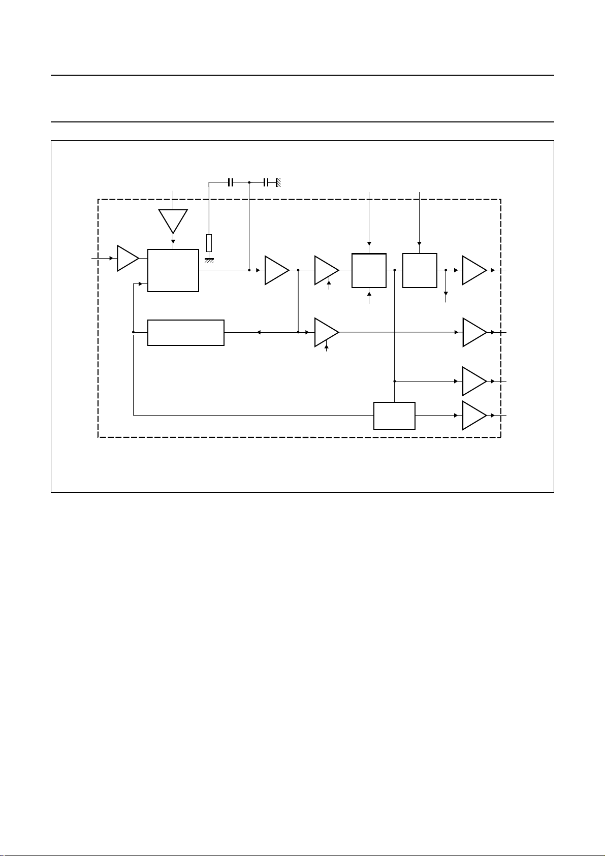
BLOCK DIAGRAM
Triple high-speed Analog-to-Digital
Converter (ADC)
Philips Semiconductors Product specification
RIN
RDEC
V
ref
GAGC
GGAINC
GIN
GDEC
BAGC
BGAINC
BIN
BDEC
TDO
TCK
ADD2
ADD1
SEN
SCL
SDA
DIS
2
I
C/3W
12
10
3
14
16
20
18
22
24
28
26
36
35
34
33
38
42
39
37
32
INTERFACE
1, 5, 30, 31, 43 , 44
50, 51, 100
SERIAL
2
I
C-BUS
OR
3-WIRE
MUX
HSYNCI
2
I
C-bus; 1-bit
(H level)
90
CLAMP
ADC
RED CHANNEL
GREEN CHANNEL
BLUE CHANNEL
TDA8752A
REGULATOR
4 2 88 97 98
PWDWN
DEC2DEC1HSYNCn.c.
CP
PLL
CZ
OUTPUTS
71 to 78
45
17
15
61 to 68
46
87
25
23
49, 52 to 58
47
84
83
81
80
92
91
93
94
FCE079
R0 to R7
ROR
GCLP
GBOT
G0 to G7
GOR
OE
BCLP
BBOT
B0 to B7
BOR
CKADCO
CKBO
CKAO
CKREFO
CKEXT
INV
COAST
CKREF
TDA8752A
Fig.1 Block diagram.
Philips Semiconductors Product specification
Triple high-speed Analog-to-Digital
Converter (ADC)
CLP RAGC CLKADC
handbook, full pagewidth
RCLP
V
ref
RIN
V
P
150
kΩ
3
kΩ
45
kΩ
DAC
5
REGISTER
FINE GAIN ADJUST
I2C-bus; 5 bits
(Fr)
MUX
CLAMP
CONTROL
AGC
V
CCAR
ADC
ADC
8
D
D ≥ R
R
1
1
COARSE GAIN ADJUST
8
7
REGISTER
2
I
C-bus; 7 bits
(Cr)
DAC
8
REGISTER
2
I
C-bus; 8 bits
(Or)
OUTPUTS
SERIAL
2
I
C-BUS
TDA8752A
ROR
8
R0 to R7
OE
RBOT
HSYNCI
RGAINC
Fig.2 Red channel diagram.
1999 Feb 24 5
MGG364
Philips Semiconductors Product specification
Triple high-speed Analog-to-Digital
Converter (ADC)
handbook, full pagewidth
CKREF
edge selector
2
I
C-bus;
1 bit
(edge)
2
I
C-bus; 1 bit
(V level)
COAST
PHASE
FREQUENCY
DETECTOR
2
I
C-bus; 5 bits
(Ip, Up, Do)
DIV N (100 to 4095)
2
I
C-bus; 12 bits (Di)
C
z
CZ CP
loop filter
2
I
C-bus;
3 bits (Z)
2 bits (VCO)
C
p
VCO
2
I
C-bus;
12 to
100 MHz
phase selector A
2
I
C-bus;
5 bits (Pa)
phase selector B
2
I
C-bus; 5 bits (Pb)
CKEXT INV
MUX
2
I
C-bus;
1 bit (Cka)
0°/180°
CLK
ADC
TDA8752A
CKADCO
CKBO
2
C-bus;
I
1 bit (Ckb)
CKAO
Fig.3 PLL diagram.
SYNCHRO
CKREFO
MGG370
1999 Feb 24 6
Philips Semiconductors Product specification
Triple high-speed Analog-to-Digital
TDA8752A
Converter (ADC)
PINNING
SYMBOL PIN DESCRIPTION
n.c. 1 not connected
DEC2 2 main regulator decoupling input
V
ref
DEC1 4 main regulator decoupling input
n.c. 5 not connected
RAGC 6 red channel AGC output
RBOT 7 red channel ladder decoupling input (BOT)
RGAINC 8 red channel gain capacitor input
RCLP 9 red channel gain clamp capacitor input
RDEC 10 red channel gain regulator decoupling input
V
CCAR
RIN 12 red channel gain analog input
AGNDR 13 red channel gain analog ground
GAGC 14 green channel AGC output
GBOT 15 green channel ladder decoupling input (BOT)
GGAINC 16 green channel gain capacitor input
GCLP 17 green channel gain clamp capacitor input
GDEC 18 green channel gain regulator decoupling input
V
CCAG
GIN 20 green channel gain analog input
AGNDG 21 green channel gain analog ground
BAGC 22 blue channel AGC output
BBOT 23 blue channel ladder decoupling input (BOT)
BGAINC 24 blue channel gain capacitor input
BCLP 25 blue channel gain clamp capacitor input
BDEC 26 blue channel gain regulator decoupling input
V
CCAB
BIN 28 blue channel gain analog input
AGNDB 29 blue channel gain analog ground
n.c. 30 not connected
n.c. 31 not connected
I2C/3W 32 selection input between I2C-bus (active HIGH) and 3-wire serial bus (active LOW)
ADD1 33 I2C-bus address control input 1
ADD2 34 I2C-bus address control input 2
TCK 35 scan test mode (active HIGH)
3 gain stabilizer voltage reference input
11 red channel gain analog power supply
19 green channel gain analog power supply
27 blue channel gain analog power supply
1999 Feb 24 7
Philips Semiconductors Product specification
Triple high-speed Analog-to-Digital
Converter (ADC)
SYMBOL PIN DESCRIPTION
TDO 36 scan test output
DIS 37 I2C-bus and 3-wire disable control input (disable at HIGH level)
SEN 38 select enable for 3-wire serial bus input (see Fig.10)
SDA 39 I2C-bus/3 W serial data input
V
DDD
V
SSD
SCL 42 I
n.c. 43 not connected
n.c. 44 not connected
ROR 45 red channel ADC output bit out of range
GOR 46 green channel ADC output bit out of range
BOR 47 blue channel ADC output bit out of range
OGNDB 48 blue channel ADC output ground
B0 49 blue channel ADC output bit 0 (LSB)
n.c. 50 not connected
n.c. 51 not connected
B1 52 blue channel ADC output bit 1
B2 53 blue channel ADC output bit 2
B3 54 blue channel ADC output bit 3
B4 55 blue channel ADC output bit 4
B5 56 blue channel ADC output bit 5
B6 57 blue channel ADC output bit 6
B7 58 blue channel ADC output bit 7 (MSB)
V
CCOB
OGNDG 60 green channel ADC output ground
G0 61 green channel ADC output bit 0 (LSB)
G1 62 green channel ADC output bit 1
G2 63 green channel ADC output bit 2
G3 64 green channel ADC output bit 3
G4 65 green channel ADC output bit 4
G5 66 green channel ADC output bit 5
G6 67 green channel ADC output bit 6
G7 68 green channel ADC output bit 7 (MSB)
V
CCOG
OGNDR 70 red channel ADC output ground
R0 71 red channel ADC output bit 0 (LSB)
40 logic I2C-bus/3 W digital power supply
41 logic I2C-bus/3 W digital ground
2
C-bus/3 W serial clock input
59 blue channel ADC output power supply
69 green channel ADC output power supply
TDA8752A
1999 Feb 24 8
Philips Semiconductors Product specification
Triple high-speed Analog-to-Digital
TDA8752A
Converter (ADC)
SYMBOL PIN DESCRIPTION
R1 72 red channel ADC output bit 1
R2 73 red channel ADC output bit 2
R3 74 red channel ADC output bit 3
R4 75 red channel ADC output bit 4
R5 76 red channel ADC output bit 5
R6 77 red channel ADC output bit 6
R7 78 red channel ADC output bit 7 (MSB)
V
CCOR
CKREFO 80 reference output clock resynchronized horizontal pulse
CKAO 81 PLL clock output 3 (in phase with reference output clock)
OGNDPLL 82 PLL digital ground
CKBO 83 PLL clock output 2
CKADCO 84 PLL clock output 1 (in phase with internal ADC clock)
V
CCO(PLL)
DGND 86 digital ground
OE 87 output enable not (when OE is HIGH, the outputs are in high-impedance)
PWDWN 88 power-down control input (IC is in power-down mode when this pin is HIGH)
CLP 89 clamp pulse input (clamp active HIGH)
HSYNC 90 horizontal synchronization input pulse
INV 91 PLL clock output inverter command input (invert when HIGH)
CKEXT 92 external clock input
COAST 93 PLL coast command input
CKREF 94 PLL reference clock input
V
CCD
AGNDPLL 96 PLL analog ground
CP 97 PLL filter input
CZ 98 PLL filter input
V
CCAPLL
n.c. 100 not connected
79 red channel ADC output power supply
85 PLL output power supply
95 digital power supply
99 PLL analog power supply
1999 Feb 24 9
Philips Semiconductors Product specification
Triple high-speed Analog-to-Digital
Converter (ADC)
handbook, full pagewidth
n.c.
DEC2
V
DEC1
n.c.
RAGC
RBOT
RGAINC
RCLP
RDEC
V
CCAR
RIN
AGNDR
GAGC
GBOT
GGAINC
GCLP
GDEC
V
CCAG
GIN
AGNDG
BAGC
BBOT
BGAINC
BCLP
BDEC
V
CCAB
BIN
AGNDB
n.c.
ref
CCA(PLL)
n.c.
V
CZCPAGNDPLL
99989796959493929190898887868584838281
100
1
2
3
4
5
6
7
8
9
10
11
12
13
14
15
16
17
18
19
20
21
22
23
24
25
26
27
28
29
30
CCD
V
CKREF
COAST
TDA8752AH
CKEXT
INV
HSYNC
CLP
PWDWNOEDGND
V
CCO(PLL)
CKADCO
CKBO
OGNDPLL
CKAO
80
79
78
77
76
75
74
73
72
71
70
69
68
67
66
65
64
63
62
61
60
59
58
57
56
55
54
53
52
51
TDA8752A
CKREFO
V
CCOR
R7
R6
R5
R4
R3
R2
R1
R0
OGNDR
V
CCOG
G7
G6
G5
G4
G3
G2
G1
G0
OGNDG
V
CCOB
B7
B6
B5
B4
B3
B2
B1
n.c.
31323334353637383940414243444546474849
n.c.
C/3W
2
I
ADD1
ADD2
TCK
TDO
DIS
SEN
SDA
DDD
V
Fig.4 Pin configuration.
1999 Feb 24 10
SSD
V
SCL
n.c.
n.c.
ROR
GOR
BOR
B0
OGNDB
50
FCE080
n.c.

Philips Semiconductors Product specification
Triple high-speed Analog-to-Digital
Converter (ADC)
FUNCTIONAL DESCRIPTION
This triple high-speed 8-bit ADC is designed to convert
RGB signals, from a PC or work station, into data used by
a LCD driver (pixel clock up to 200 MHz, using 2 ICs).
IC analog video inputs
The video inputs are internally DC polarized. These inputs
are AC coupled externally.
Clamps
Three independent parallel clamping circuits are used to
clamp the video input signals on the black level and to
control the brightness level. The clamping code is
programmable between code −63.5 and +64 in steps of
1
⁄2LSB. The programming of the clamp value is achieved
via an 8-bit DAC. Each clamp must be able to correct an
offset from±0.1 V to±10 mV within 300 ns, and correct the
total offset in 10 lines.
The clamps are controlled by an external TTL positive
going pulse (pin CLP). The drop of the video signal is
<1 LSB.
Normally, the circuit operates with a 0 code clamp,
corresponding to the 0 ADC code. This clamp code can be
changed from −63.5 to +64 as represented in Fig.7, in
steps of1⁄2LSB. The digitized video signal is always
between code 0 and code 255 of the ADC.
TDA8752A
The output of the multiplexer is either the normal video
signal or the 0.156 V reference signal (during HSYNC).
The corresponding ADC outputs are then compared to a
pre-set value loaded in a register. Depending on the result
of the comparison, the gain of the variable gain amplifiers
is adjusted (coarse gain control; see Figs 2 and 8).
The three 7-bit registers receive data via a serial interface
to enable the gain to be programmed.
The pre-set value loaded in the 7-bit register is chosen
between approximately 67 codes to ensure the full-scale
input range (see Fig.8). A contrast control can be achieved
using these registers. In this case care should be taken to
stay within the allowed code range (32 to 99).
A fine correction using three 5-bit DACs, also controlled via
the serial interface, is used to finely tune the gain of the
three channels (fine gain control; see Figs 2 and 9) and to
compensate the channel-to-channel gain mismatch.
With a full scale ADC input, the resolution of the fine
register corresponds to
To use these gain controls correctly, it is recommended to
fix the coarse gain (to have a full-scale ADC input signal)
to within 4 LSB and then adjust it with the fine gain.
The gain is adjusted during HSYNC. During this time the
output signal is not related to the amplified input signal.
The outputs, when the coarse gain system is stable, are
related to the programmed coarse code (see Fig.8).
1
⁄2LSB peak-to-peak variation.
Variable gain amplifier
Three independent variable gain amplifiers are used to
provide, to each channel, a full-scale input range signal to
the 8-bit ADC. The gain adjustment range is designed so
that, for an input range varying from 0.4 to 1.2 V (p-p), the
output signal corresponds to the ADC full-scale input of
1 V (p-p).
To ensure that the gain does not vary over the whole
operating temperature range, an external reference of
2.5 V DC, (V
supplied externally, is used to calibrate the gain at the
beginning of each video line before the clamp pulse using
the following principle.
A differential of 0.156 V (p-p) (1⁄16V
generated internally from the reference voltage (V
During the synchronization part of the video line, the
multiplexer, controlled by the TTL synchronization signal
(HSYNCI, coming from HSYNC; see Fig.1) with a width
equal to one of the video synchronization signals
(e.g. signal coming from a synchronization separator), is
switched between the two amplifiers.
1999 Feb 24 11
with a 100 ppm/°C maximum variation)
ref
) reference signal is
ref
ref
).
ADCs
The ADCs are 8-bit with a maximum clock frequency of
100 Msps. The ADCs input range is 1 V (p-p) full-scale.
One out of range bit exists per channel (ROR, GOR and
BOR). It will be at logic 1 when the signal is out of range
the full scale of the ADCs.
Pipeline delay in the ADCs is 1 clock cycle from sampling
to data output.
The ADCs reference ladders regulators are integrated.
ADC outputs
ADC outputs are straight binary. An output enable pin
(
OE; active LOW) enables the output status between
active and high-impedance (OE = HIGH) to be switched;
it is recommended to load the outputs with a 10 pF
capacitive load. The timing must be checked very carefully
if the capacitive load is more than 10 pF.
 Loading...