

Philips tda8752 DATASHEETS
INTEGRATED CIRCUITS
DATA SH EET
TDA8752
Triple high speed Analog-to-Digital
Converter (ADC) for LCD drive
Objective specification
File under Integrated Circuits, IC02
1996 Sep 12

Philips Semiconductors Objective specification
Triple high speed Analog-to-Digital
Converter (ADC) for LCD drive
FEATURES
• Triple 8-bit ADC
• Sampling rate up to 80 MHz
• IC controllable via a serial interface, which can be either
I2C-bus or 3-wire, selected via a TTL input pin
• IC analog voltage input from 0.4 to 1.2 V (p-p) to
produce full-scale ADC input of 1 V (p-p)
• 3 clamps for programming a clamping code between
−63.5 and +64 in steps of1⁄2LSB
• 3 controllable amplifiers: gain controlled via the serial
interface to produce a full scale resolution of
peak-to-peak
• Amplifier bandwidth of 250 MHz
• Low gain variation with temperature
• PLL, controllable via the serial interface to generate the
ADC clock, which can be locked to a line frequency from
15 to 280 kHz
• Integrated PLL divider
• Programmable phase clock adjustment cells
• Internal voltage regulators
• TTL compatible digital inputs and outputs
• Chip enable high-impedance ADC output
• Power-off mode
• Possibility to use up to four ICs in the same system,
using the I2C-bus interface, or more, using the 3-wire
serial interface
• 1 W power dissipation.
1
⁄2LSB
TDA8752
GENERAL DESCRIPTION
The TDA8752 is a triple 8-bit ADC with controllable
amplifiers and clamps for the digitizing of large bandwidth
RGB signals.
The clamp level, the gain and all of the other settings are
controlled via a serial interface (either I
serial bus, selected via a logic input). The amplifiers are
optimized for stability as a function of temperature
variations.
The IC also includes a PLL that can be locked on the
horizontal line frequency and generates the ADC clock.
The PLL jitter is minimized for high resolution PC graphics
applications. An external clock can also be input to the
ADC.
It is possible to set the TDA8752 serial bus address
between four fixed values, in the event that several
TDA8752 ICs are used in a system, using the I
interface (for example, two ICs used in an odd/even
configuration).
2
C-bus or 3-wire
2
C-bus
APPLICATIONS
• R, G and B high speed digitizing
• LCD panels drive
• LCD projection systems
• VGA and higher resolutions
• Using two ICs in parallel, higher display resolution can
be obtained; 160 MHz pixel frequency.
ORDERING INFORMATION
TYPE
NUMBER
TDA8752H/6
TDA8752H/8 80
1996 Sep 12 2
NAME DESCRIPTION VERSION
QFP100
plastic quad flat package; 100 leads (lead length 1.95 mm);
body 14 × 20 × 2.8 mm
PACKAGE SAMPLING
FREQUENCY
(MHZ)
SOT317-2
60

Philips Semiconductors Objective specification
Triple high speed Analog-to-Digital
TDA8752
Converter (ADC) for LCD drive
QUICK REFERENCE DATA
SYMBOL PARAMETER CONDITIONS MIN. TYP. MAX. UNIT
V
CCA
V
DDD
V
CCD
V
CCO
V
CCA(PLL)
V
CCO(PLL)
I
CCA
I
DDD
I
CCD
I
CCO
I
CCA(PLL)
I
CCO(PLL)
f
CLK
f
ref(PLL)
f
VCO
INL DC integral non linearity full-scale; ramp input;
DNL DC differential non linearity full-scale; ramp input;
/T amplifier gain stability as a
∆G
amp
B amplifier bandwidth −3 dB; T
t
set
j
PLL(rms)
DR
PLL
P
tot
analog supply voltage for R, G and B channels 4.75 5.0 5.25 V
logic supply voltage for I2C-bus and 3-wire 4.75 5.0 5.25 V
digital supply voltage 4.75 5.0 5.25 V
output stages supply voltage for R, G and B channels 4.75 5.0 5.25 V
analog PLL supply voltage 4.75 5.0 5.25 V
output PLL supply voltage 4.75 5.0 5.25 V
analog supply current − 120 − mA
logic supply current for I2C-bus and 3-wire − 1.0 − mA
digital supply current − 40 − mA
output stages supply current f
= 80 MHz; ramp input − 6 − mA
clk
analog PLL supply current − 28 − mA
output PLL supply current − 5 − mA
maximum clock frequency TDA8752/6 60 −−MHz
TDA8752/8 80 −−MHz
PLL reference clock frequency 15 − 280 kHz
VCO output clock frequency 12 − 80 MHz
−±0.5 tbf LSB
= 80 MHz
f
clk
−±0.5 tbf LSB
f
= 80 MHz
clk
V
function of temperature
settling time of the ADC block
plus AGC
maximum PLL phase jitter
= 2.5 V with
ref
100 ppm/°C maximum
=25°C 250 −−MHz
amb
input signal settling
time < 1 ns; T
amb
=25°C
−−200 ppm/°C
−−6ns
− 0.2 − ns
(RMS value)
PLL divider ratio without divide-by-2 15 − 2047
total power consumption f
= 80 MHz;
CLK
− 1.0 tbf W
ramp input
1996 Sep 12 3
Philips Semiconductors Objective specification
Triple high speed Analog-to-Digital
Converter (ADC) for LCD drive
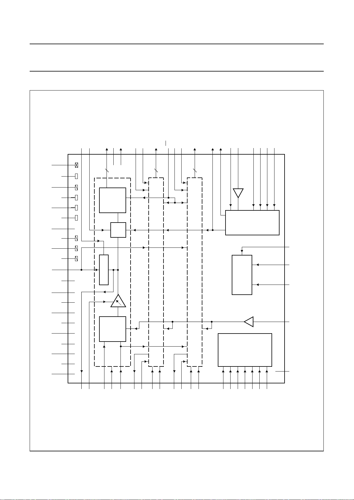
BLOCK DIAGRAM
RBOT
DGND
AGNDPLL
OGNDG
SSD
V
AGNDG
book, full pagewidth
CLP
CCA(PLL)
V
CCOB
V
CCOR
V
CCAB
V
CCAR
V
86
82
96
OGNDPLL
48
OGNDB
60
70
OGNDR
41
29
AGNDB
21
13
AGNDR
89
85
CCO(PLL)
99
V
95
CCD
V
59
69
CCOG
V
79
40
DDD
V
27
19
CCAG
V
11
RCLP
9
6
TCK
TDO
R0 to R7
7
8
35
71 to 78
CLAMP
12
10
36
OUTPUTS
ADC
MUX
3
GBOT
GCLP
17
15
RED CHANNEL
14
16
BCLP
OE
G0 to G7
87
25
23
61 to 68
GREEN CHANNEL
22
20
18
24
BBOT
B0 to B7
49,
52 to 58
BLUE CHANNEL
28
26
CKAOUT
84
CKBOUT
83
TDA8752
HSYNCI
COAST
CKREF
94
C-bus; 1-bit
2
I
(V level)
COASTI
REGULATOR
C-BUS
2
SERIAL
I
INTERFACE
3334384239
CKEXT
929391
PLL
OR
3-WIRE
C-bus; 1-bit
2
I
37
CP
CZ
INV
98
97
(H level)
1, 5, 30, 31, 43 to 47,
32
TDA8752
MGG363
PWOFF
DEC2DEC1HSYNCn.c.
4288
Fig.1 Block diagram.
90
50, 51, 80, 81, 100
1996 Sep 12 4
RAGC
RGAINC
RIN
RDEC
ref
V
GAGC
GIN
GGAINC
GDEC
BAGC
BIN
BGAINC
BDEC
ADD1
ADD2
SEN
SCL
DIS
SDA
C/3W
2
I
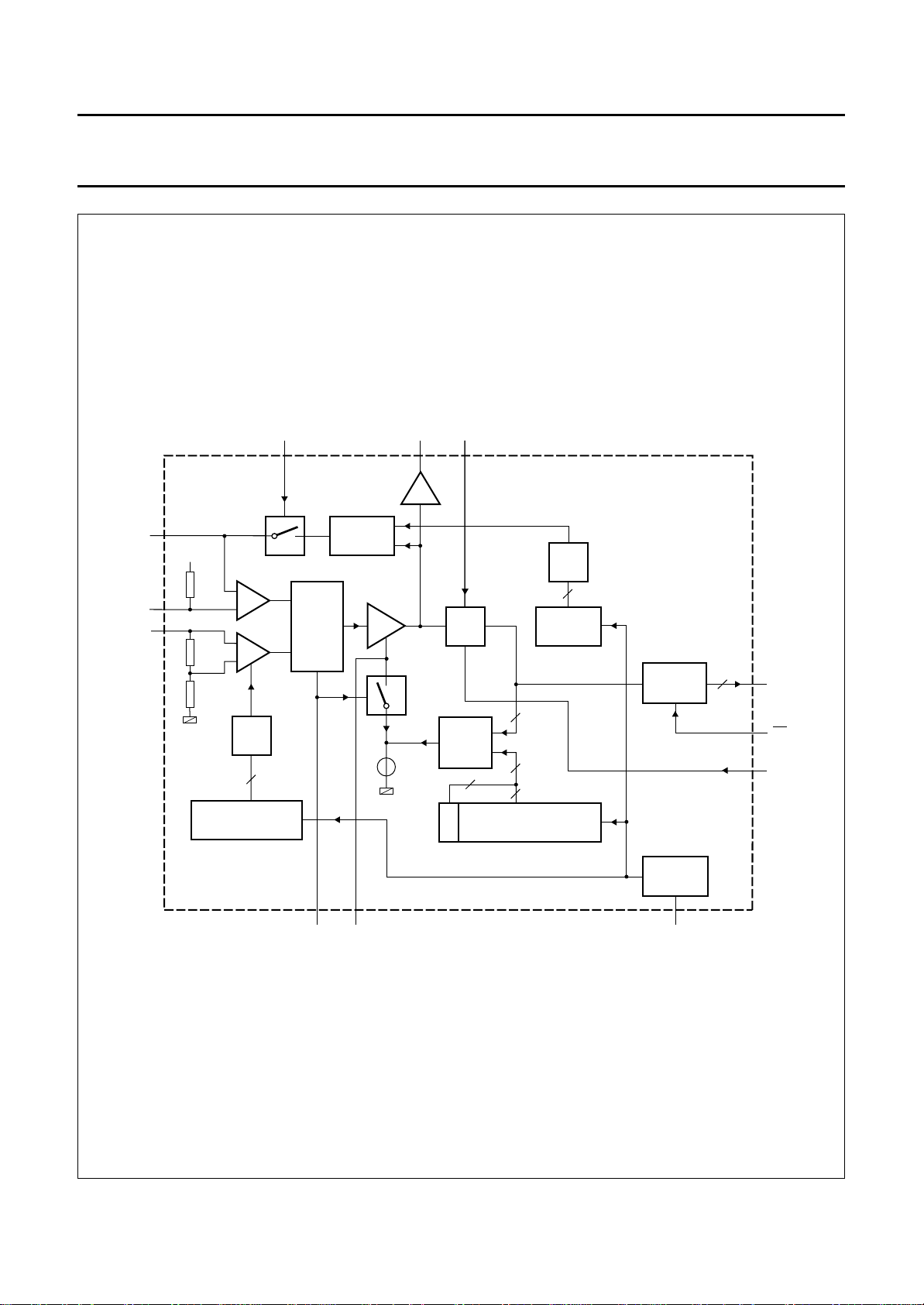
Philips Semiconductors Objective specification
Triple high speed Analog-to-Digital
Converter (ADC) for LCD drive
handbook, full pagewidth
RCLP
RIN
V
ref
V
P
150
kΩ
CLP RAGC CKAOUT
CLAMP
CONTROL
MUX
AGC
ADC
ADC
DAC
8
REGISTER
2
I
C-bus; 8 bits
(OR, OG, OB)
OUTPUTS
TDA8752
8
R0 to R7
DAC
5
REGISTER
FINE GAIN ADJUST
I2C-bus; 5 bits
(FR, FG, FB)
HSYNCI
D
D ≥ R
R
1
1
COARSE GAIN ADJUST
RGAINC
Fig.2 Red channel diagram.
8
8
7
REGISTER
2
I
C-bus; 7 bits
(CR, CG, CB)
SERIAL
2
I
OE
RBOT
C-BUS
MGG364
1996 Sep 12 5
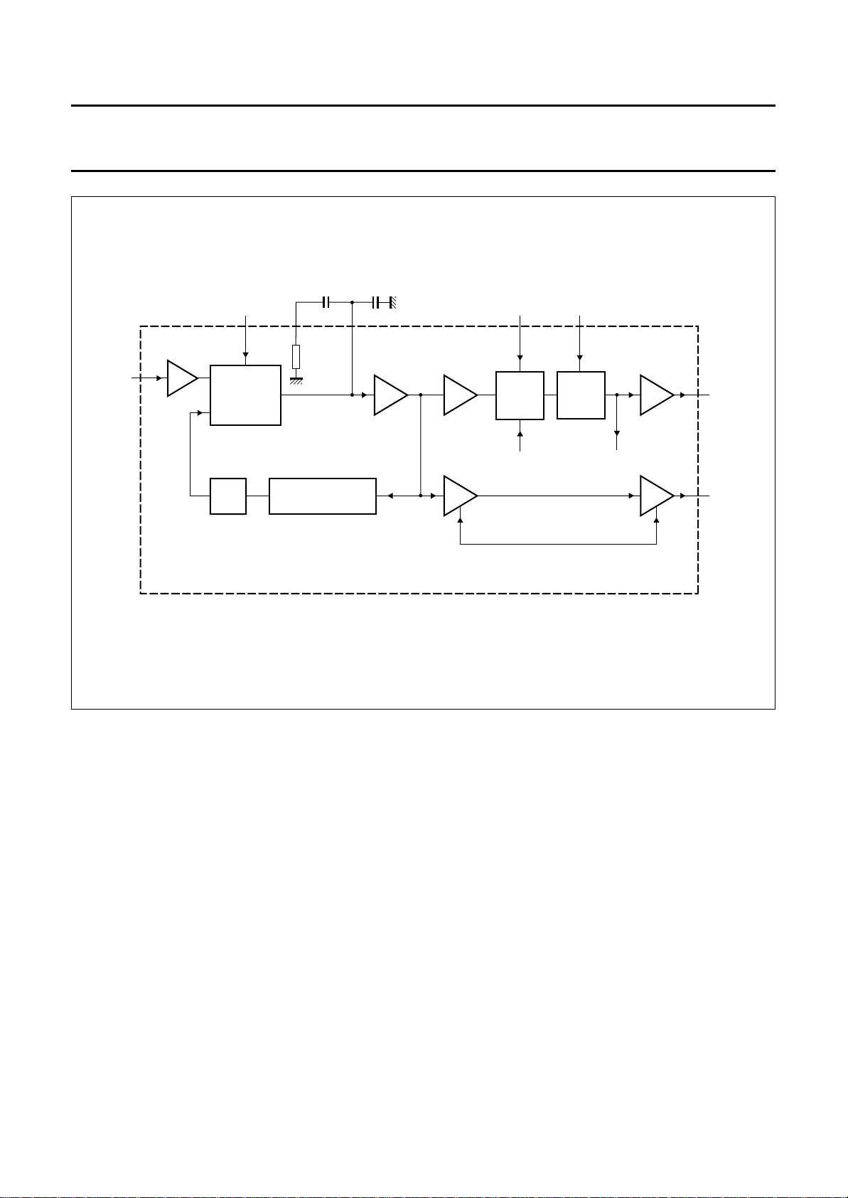
Philips Semiconductors Objective specification
Triple high speed Analog-to-Digital
Converter (ADC) for LCD drive
C
handbook, full pagewidth
CKREF
2
I
C-bus;
1 bit
(edge)
COAST
PHASE
FREQUENCY
DETECTOR
2
I
C-bus; 5 bits
(IP, UP, DO)
÷ 2
DIV N (15 to 2047)
2
I
C-bus; 11 bits
(Di)
z
CZ CP
loop filter
2
I
C-bus;
3 bits (Z)
C
p
VCO
2
I
C-bus;
2 bits
(VCO)
phase selector B
2
I
(Pb)
phase selector A
2
I
(Pa)
C-bus; 5 bits
12 to
80 MHz
C-bus; 5 bits
disable
2
I
C-bus; 1 bit
(Ckb)
CKEXT INV
MUX
2
I
C-bus; 1 bit
(Cka)
0° / 180°
TDA8752
CKAOUT
CLK
ADC
CKBOUT
MGG370
Fig.3 PLL diagram.
1996 Sep 12 6
Philips Semiconductors Objective specification
Triple high speed Analog-to-Digital
TDA8752
Converter (ADC) for LCD drive
PINNING
SYMBOL PIN DESCRIPTION
n.c. 1 not connected
DEC2 2 main regulator decoupling input
V
ref
DEC1 4 main regulator decoupling input
n.c. 5 not connected
RAGC 6 red channel AGC output
RBOT 7 red channel ladder decoupling input (BOT)
RGAINC 8 red channel gain capacitor input
RCLP 9 red channel gain clamp capacitor input
RDEC 10 red channel gain regulator decoupling input
V
CCAR
RIN 12 red channel gain analog input
AGNDR 13 red channel gain analog ground
GAGC 14 green channel AGC output
GBOT 15 green channel ladder decoupling input (BOT)
GGAINC 16 green channel gain capacitor input
GCLP 17 green channel gain clamp capacitor input
GDEC 18 green channel gain regulator decoupling input
V
CCAG
GIN 20 green channel gain analog input
AGNDG 21 green channel gain analog ground
BAGC 22 blue channel AGC output
BBOT 23 blue channel ladder decoupling input (BOT)
BGAINC 24 blue channel gain capacitor input
BCLP 25 blue channel gain clamp capacitor input
BDEC 26 blue channel gain regulator decoupling input
V
CCAB
BIN 28 blue channel gain analog input
AGNDB 29 blue channel gain analog ground
n.c. 30 not connected
n.c. 31 not connected
I2C/3W 32 selection input between I2C-bus (active LOW) and 3-wire serial bus (active HIGH)
ADD2 33 I
ADD1 34 I2C-bus address control input 1
TCK 35 scan test mode (active HIGH)
3 gain stabilizer voltage reference input
11 red channel gain analog power supply
19 green channel gain analog power supply
27 blue channel gain analog power supply
2
C-bus address control input 2
1996 Sep 12 7
Philips Semiconductors Objective specification
Triple high speed Analog-to-Digital
Converter (ADC) for LCD drive
SYMBOL PIN DESCRIPTION
TDO 36 scan test output
DIS 37 I2C/3W disable control input
SEN 38 select enable for 3-wire serial bus input
SDA 39 I2C/3W serial data input
V
DDD
V
SSD
SCL 42 I2C/3W serial clock input
n.c. 43 not connected
n.c. 44 not connected
n.c. 45 not connected
n.c. 46 not connected
n.c. 47 not connected
OGNDB 48 blue channel ADC output ground
B0 49 blue channel ADC output bit 0 (LSB)
n.c. 50 not connected
n.c. 51 not connected
B1 52 blue channel ADC output bit 1
B2 53 blue channel ADC output bit 2
B3 54 blue channel ADC output bit 3
B4 55 blue channel ADC output bit 4
B5 56 blue channel ADC output bit 5
B6 57 blue channel ADC output bit 6
B7 58 blue channel ADC output bit 7 (MSB)
V
CCOB
OGNDG 60 green channel ADC output ground
G0 61 green channel ADC output bit 0 (LSB)
G1 62 green channel ADC output bit 1
G2 63 green channel ADC output bit 2
G3 64 green channel ADC output bit 3
G4 65 green channel ADC output bit 4
G5 66 green channel ADC output bit 5
G6 67 green channel ADC output bit 6
G7 68 green channel ADC output bit 7 (MSB)
V
CCOG
OGNDR 70 red channel ADC output ground
R0 71 red channel ADC output bit 0 (LSB)
40 logic I2C/3W digital power supply
41 logic I2C/3W digital ground
59 blue channel ADC output power supply
69 green channel ADC output power supply
TDA8752
1996 Sep 12 8
Philips Semiconductors Objective specification
Triple high speed Analog-to-Digital
Converter (ADC) for LCD drive
SYMBOL PIN DESCRIPTION
R1 72 red channel ADC output bit 1
R2 73 red channel ADC output bit 2
R3 74 red channel ADC output bit 3
R4 75 red channel ADC output bit 4
R5 76 red channel ADC output bit 5
R6 77 red channel ADC output bit 6
R7 78 red channel ADC output bit 7 (MSB)
V
CCOR
n.c. 80 not connected
n.c. 81 not connected
OGNDPLL 82 PLL digital ground
CKBOUT 83 PLL clock output 2
CKAOUT 84 PLL clock output 1 (in phase with internal ADC clock)
V
CCO(PLL)
DGND 86 digital ground
OE 87 output enable not (when OE is HIGH, the outputs are in high-impedance)
PWOFF 88 power off control input (IC is in power off mode when this pin is HIGH)
CLP 89 clamp pulse input
HSYNC 90 horizontal synchronization input pulse
INV 91 PLL clock output inverter command input
CKEXT 92 external clock input
COAST 93 PLL coast command input
CKREF 94 PLL reference clock input
V
CCD
AGNDPLL 96 PLL analog ground
CP 97 PLL filter input
CZ 98 PLL filter input
V
CCAPLL
n.c. 100 not connected
79 red channel ADC output power supply
85 PLL output power supply
95 digital power supply
99 PLL analog power supply
TDA8752
1996 Sep 12 9
 Loading...