

Philips TDA8745-N2, TDA8745H-N2 Datasheet

DATA SH EET
Preliminary specification
Supersedes data of 1995 Mar 08
File under Integrated Circuits, IC02
1996 Mar 11
INTEGRATED CIRCUITS
TDA8745
Satellite sound receiver with
I
2
C-bus control

1996 Mar 11 2
Philips Semiconductors Preliminary specification
Satellite sound receiver with I2C-bus control
TDA8745
FEATURES
• On-chip frequency synthesizer and mixer:
– tuning range 4 to 9.77 MHz
– reference oscillator 4 MHz (using a crystal or 4 MHz
frequency source)
• IF input switches allowing selection of various IF
bandwidths (wide or narrow)
• Demodulation of two audio signals by wide band
Phase-Locked Loops (PLLs)
• Audio level control after PLL (modulation depth setting)
• Noise Reduction (NR) bypass for use with main audio
signals
• Left, right and mono output [1⁄2(l + r)] on SCART level
• External audio inputs (for decoder connection)
• Selectable de-emphasis (DEEM) 50 µs, 75 µs, J17 and
flat response
• I2C-bus control of all functions
• Two selectable addresses
• Carrier presence detector with automatic mute option.
APPLICATIONS
• Satellite receivers
• TV sets
• Video recorders.
GENERAL DESCRIPTION
The TDA8745 is the successor of the TDA8740 and
TDA8741. The device contains the functionality of the
TDA8740 and TDA8741 together with a synthesizer, mixer
and I
2
C-bus control.
The pin numbers mentioned in this publication refer to the
SDIP42 package; unless otherwise indicated.
ORDERING INFORMATION
TYPE
NUMBER
PACKAGE
NAME DESCRIPTION VERSION
TDA8745 SDIP42
plastic shrink dual in-line package; 42 leads (600 mil)
SOT270-1
TDA8745H QFP44
plastic quad flat package; 44 leads (lead length 1.3 mm);
body 10 × 10 × 1.75 mm
SOT307-2

1996 Mar 11 3
Philips Semiconductors Preliminary specification
Satellite sound receiver with I2C-bus control
TDA8745
QUICK REFERENCE DATA
SYMBOL PARAMETER CONDITIONS MIN. TYP. MAX. UNIT
V
P1
synthesizer and mixer supply voltage 4.5 5.0 5.5 V
V
P2
I2C-bus supply voltage 4.5 5.0 5.5 V
V
P3
general supply voltage 8.0 12.0 13.2 V
I
P1
synthesizer and mixer supply current − 37 48 mA
I
P2
I2C-bus supply current − 0.6 − mA
I
P3
general supply current − 35 46 mA
S/N(A) signal-to-noise ratio secondary channel A-weighted;
NR = on; DEEM = 75 µs
68 77 − dB
V
i(rms)
input sensitivity (RMS value) baseband input
to mixer
S/N(A) = 40 dB;
NR = on; DEEM = 75 µs
− 0.5 1.5 mV
V
i(rms)
baseband input voltage (RMS value) THD ≤ 0.5% 200 mV
V
o
output voltage −8 −6 −4 dBV
P
tot
total power dissipation − 610 800 mW
T
stg
storage temperature −65 − +150 °C
T
amb
operating ambient temperature −20 − +70 °C
1996 Mar 11 4
Philips Semiconductors Preliminary specification
Satellite sound receiver with I2C-bus control
TDA8745
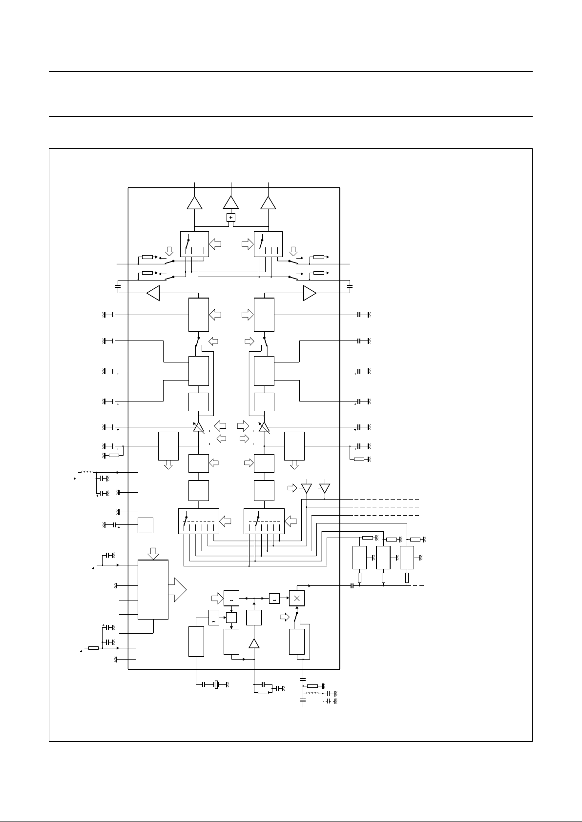
BLOCK DIAGRAM
handbook, full pagewidth
ϕ
MBE037
330 Ω
330 Ω
330
Ω
330 Ω
330 Ω
1 kΩ
470
kΩ
1
µF
HF
LIMITER
PLL
HF
LIMITER
PLL
IL2 to IL0
IR2 to IR0
PRESENCE
DETECTOR
AUDIO
LPF
NOISE
REDUCTION
OMR
12 to 3dB
LEV3 to LEV0
OML
PRESENCE
DETECTOR
BB
DC
DC
PDR
IL2
IR2
PRES DET R
C
DC R
RECT
R
C
NR D R
C
D R
DEEM OUT LDEEM OUT R
C
ATT/REC R
PDL
9
PE
11 13 15 7 8
10.7
NARROW
5
330
Ω
10 nF
10
µF
DE-EMPHASIS
50 µs
J17
10
µF
1
µF
4.7
nF
10
nF
75 µs
220 nF
AUDIO
LPF
NOISE
REDUCTION
DE-EMPHASIS
50
flat
flat µs
J17
75 µs
DEM1 and DEM0 OS1 and OS0NR
OML
OMR
O
L
O
M
O
R
23
21
22
29
30 31
24
27
26 2839 1
35 34 33 2537 38 36
EXT
L
C
D L
C
CL L
C
CL L
C
NR D L
C
DC L
V
ref
V
P3
V
P2
V
P1 AFGNDHFGND
PRES DET L
C
ATT/REC L
RECT
L
EXT
470
kΩ
1
µF
12 to 3dB
10
µF
4241
10
µF
1
µF
4.7
nF
10
nF
220 nF
203210
2.2
µF
19
V
ref
1614171812
2
PDL
PDR
I C
INTERFACE
2
VCO
frequency
synthesizer
30 to 40 MHz
N
2
CHARGE
PUMP
200
CRYSTAL
OSCILLATOR
PRE-BPF
4 MHz
MIXER
BPFN
TUN9 to TUN0
SDA
5 V
SCL
ADD
sel
I CGND
46
SYNGND
XTAL
2
40
BASEBAND
IN
IF OUT
6.8
kΩ
33
nF
3
27 pF
27 pF
27 pF
15 pF
1 µF
1000 µF
10
pF
4 MHz
10.52
NARROW
10.7
WIDE
SLF
IN-1
IN-2
IN-3
IN-4
IN-5
IN-6
R
TDA8745
(2)
(1)
(2)
(2)
47 µH
100 µH
4.7 Ω
22
nF
12 V
100 µF
22
nF
5 V
22
nF
Fig.1 Block diagram (SDIP42).
When driving more than three filters in parallel, pin 5 should be buffered.
(1) Add 15 pF for NTSC.
(2) Ceramic filters:
SFE10.7MJA10-A (narrow)
SFE10.52MJA10-A (narrow)
SFE10.7MS2-A (wide).

1996 Mar 11 5
Philips Semiconductors Preliminary specification
Satellite sound receiver with I2C-bus control
TDA8745
PINNING
SYMBOL
PIN
DESCRIPTION
SDIP42 QFP44
C
DC R
1 39 DC decoupling capacitor (right channel)
SLF 2 41 synthesizer loop-filter
BASEBAND IN 3 42 baseband input to mixer
V
P1
4 43 synthesizer and mixer supply voltage (+5 V)
IF OUT 5 44 intercarrier output from mixer
SYNGND 6 1 synthesizer and mixer ground
IN-5 7 2 intercarrier input 5/port expansion output 1
IN-6 8 3 intercarrier input 6/port expansion output 2
IN-1 9 4 Intercarrier input 1
HFGND 10 5 HF ground
IN-2 11 6 intercarrier input 2
ADD
sel
12 7 I2C-bus address selection
IN-3 13 8 Intercarrier input 3
I
2
CGND 14 9 I2C-bus ground
IN-4 15 10 intercarrier input 4
V
P2
16 11 I2C-bus supply voltage (+5 V)
SCL 17 12 I
2
C-bus serial clock input
SDA 18 13 I
2
C-bus serial data input/output
V
ref
19 14 decoupling capacitor for reference voltage
V
P3
20 15 general supply voltage (+12 V)
O
M
21 17 mono channel output [1⁄2(l + r)]
O
R
22 18 right channel output
O
L
23 19 left channel output
EXT
R
24 20 external audio input (right channel)
EXT
L
25 21 external audio input (left channel)
C
ATT/RECR
26 22 attack/recovery capacitor (right channel)
RECT
R
27 23 rectifier DC decoupling (right channel)
C
NR D R
28 24 noise reduction de-emphasis capacitor (right channel)
C
DR
29 25 de-emphasis capacitor (right channel)
DEEM OUT R 30 26 de-emphasis output (right channel)
C
CL R
31 27 audio pass-through input (right channel)
AFGND 32 28 AF ground
C
CL L
33 29 audio pass-through input (left channel)
DEEM OUT L 34 30 de-emphasis output (left channel)
C
DL
35 31 de-emphasis capacitor (left channel)
C
NR D L
36 32 noise reduction de-emphasis capacitor (left channel)
RECT
L
37 33 rectifier DC decoupling (left channel)
C
ATT/RECL
38 34 attack/recovery capacitor (left channel)
1996 Mar 11 6
Philips Semiconductors Preliminary specification
Satellite sound receiver with I2C-bus control
TDA8745
PRES DET R 39 35 presence detector timing (right channel)
XTAL 40 36 crystal input for 4 MHz oscillator
PRES DET L 41 37 presence detector timing (left channel)
C
DC L
42 38 DC decoupling capacitor (left channel)
n.c. − 16 not connected
n.c. − 40 not connected
SYMBOL
PIN
DESCRIPTION
SDIP42 QFP44
handbook, halfpage
1
2
3
4
5
6
7
8
9
10
11
12
13
40
39
38
37
36
35
34
33
32
31
30
29
28
27
14
15
16
17
18
19
20
22
23
24
25
26
21
42
41
O
O
EXT
EXT
ATT/REC R
DEEM OUT R
AFGND
RECT
PRES DET R
XTAL
DC L
DC R
ATT/REC L
PRES DET LSLF
BASEBAND IN
IF OUT
SYNGND
IN-5
IN-6
IN-1
HFGND
IN-2
ADD
IN-3
I CGND
IN-4
SCL
SDA
V
P3
V
P2
V
P1
V
M
O
DEEM OUT L
RECT
TDA8745
2
ref
MBE035
C
C
L
C
NR D L
C
D L
C
CL L
C
CL R
C
D R
C
C
NR D R
R
L
R
L
R
sel
C
Fig.2 Pin configuration (SDIP42).
1996 Mar 11 7
Philips Semiconductors Preliminary specification
Satellite sound receiver with I2C-bus control
TDA8745
Fig.3 Pin configuration (QFP44).
handbook, full pagewidth
1
2
3
4
5
6
7
8
9
10
11
33
32
31
30
29
28
27
26
25
24
23
12
13
14
15
16
17
18
19
20
21
22
44
43
42
41
40
39
38
37
36
35
34
RECT
NR D L
DEEM OUT L
AFGND
DEEM OUT R
C
C
RECT
IF OUTVBASEBAND IN
SLF
n.c.
DC L
C
DC R
P1
C
XTAL
PRES DET R
PRES DET L
ATT/REC L
C
TDA8745H
SYNGND
IN-5
IN-6
IN-1
HFGND
IN-2
ADD
IN-3
IN-4
V
2
I CGND
SCL
SDA
V
O
M
O
R
O
R
C
L
n.c.
EXTLEXT
ATT/REC R
ref
V
P3
MBE034
L
C
CL L
C
CL R
D R
R
NR D R
C
D L
C
sel
P2

1996 Mar 11 8
Philips Semiconductors Preliminary specification
Satellite sound receiver with I2C-bus control
TDA8745
FUNCTIONAL DESCRIPTION
Satellite sound
The baseband signal coming from a satellite tuner
comprises the demodulated video signal plus a number of
sound carriers in the event of reception of a PAL, NTSC or
SECAM satellite signal.
Nearest to the video signal is the main sound carrier which
carries the mono sound related to the video. This is an FM
modulated carrier with a fixed pre-emphasis. The carrier
frequency can be in the range of 5.8 to 6.8 MHz.
Additionally, a number of optional secondary sound
carriers may be present. These can be used for stereo or
multi-language sound related to the video signal, or for
unrelated radio sound. These carriers are also FM
modulated, and for better sound quality (improved
signal-to-noise performance) broadcast satellites
(e.g. ‘ASTRA’) use a noise reduction system (adaptive
pre-emphasis circuit, combined with a fixed
pre-emphasis). These secondary carrier frequencies can
be in the range of 6.30 to 8.28 MHz.
For accurate tuning to the many sound carriers, an internal
frequency synthesizer and mixer are used to transfer the
sound carriers to intermediate frequencies of
10.7 and 10.52 MHz.
The TDA8745 contains all circuitry for the processing of
the main channel and secondary channels, from baseband
signal to line (SCART) output drivers. By means of
external band-pass filters the desired frequencies coming
from the synthesizer/mixer are routed to the IF
limiter/demodulator inputs.
Band-pass filter and mixer
Before the incoming baseband signal is applied to the
mixer, the signal is filtered. Related to the sound carriers,
the level of the video part of the baseband signal can be
much higher, so to avoid overload it is desirable to
attenuate the latter, this is also to avoid interference
(additional unwanted mix of signals after mixing).
The internal band-pass filter (pass band from
approximately 4 to 10 MHz) is completed by a simple
external notch filter. The external filter provides substantial
attenuation of the video colour carrier. The notch filter is
chosen to be external because the required notch
frequency is TV standard dependent and also because an
accurate on-chip notch filter requires a tuning mechanism
(consuming additional chip area).
The mixer is a double-balanced mixer with degeneration,
this to accommodate the level of the filter output signal.
The mixer transfers the different sound carrier frequencies
to fixed intermediate frequencies of 10.7 and 10.52 MHz.
These frequencies are fed via an internal buffer stage to
external ceramic band-pass filters before they are routed
to the two demodulator inputs. The buffer stage can drive
up to three external ceramic band-pass filters (assuming
330 Ω filter terminations) but this can be increased to four
or more by adding an external buffer.
Synthesizer
The synthesizer consists of the following parts:
• Reference oscillator
• Reference divider
• A 10-bit programmable divider
• Phase detector
• Charge pump
• Voltage Controlled Oscillator (VCO)
• Divide-by-two circuit.
The reference frequency circuit consists of a 4 MHz crystal
oscillator and a divider (by 200). The resulting reference
frequency of 20 kHz is fed to the phase detector.
The programmable divider consists of a series of cells
(divide by 2 or 3) connected as a ripple counter.
The minimum division ratio is 2
n
and the maximum division
ratio is 2
n+1
−1.
The programmable divider output signal is also fed to the
phase detector. The charge pump provides output current
pulses in accordance with the signals from the phase
detector. The final tuning voltage for the VCO is provided
by the loop filter and a buffer amplifier.
The oscillator frequency range is from
29.04 to 40.94 MHz, depending on the setting of the
programmable divider (by the TUN signal). The tuning
voltage is clipped to limit the VCO frequency range.
The frequency of the oscillator is divided-by-two before it
is applied to the mixer (to obtain the desired 10 kHz
resolution).
Left and right channel inputs
A maximum of six inputs are available (pins 9, 11, 13, 15,
7 and 8). External ceramic band-pass filters, which are
tuned to the desired intermediate frequencies, route the
signals to the inputs.
For stereo purposes the TDA8745 contains two identical
secondary sound processing channels (secondary
channel 1 will also be referred to as ‘left’ or ‘language 1’
and secondary channel 2 as ‘right’ or ‘language 2’).

1996 Mar 11 9
Philips Semiconductors Preliminary specification
Satellite sound receiver with I2C-bus control
TDA8745
With the input selection every input pin of the left and/or
right channel can be independently selected. Input
selection for the left channel is controlled by the IL signal
and for the right channel by the IR signal.
From the inputs, the signals are coupled to the
limiter/amplifier and to the PLL demodulator of each
channel. The output signal from the PLL is routed to both
the presence detector and audio level control.
The inputs of pins 7 and 8 can be changed into digital
outputs for external switching purposes, set by the so
called Port Extension bit (PE). Not used inputs should be
connected to ground. Note that the inputs of pins 7 and 8
are also floating when not in Port Extension mode.
Presence detector
The presence detector is used to determine if a carrier is
present on the channel of interest. It does so by measuring
the amount of high frequency noise (>20 kHz) in the audio
signal, which is directly related to the C/N (carrier-to-noise
ratio) at the IF input. If a carrier is present, these high
frequencies are fairly moderate, if no carrier is present,
strong noise components are present.
The audio signal, first high-pass filtered and then rectified,
is filtered by the components at pins 41 and 39
(PRES DET L and PRES DET R). The DC level at this pin
is then compared with an internal reference voltage. If the
level at pins 41 and 39 exceeds this voltage level, the
presence detector output goes HIGH (no carrier).
This output signal can be used to drive the output mute (if
bit PDM = 1; see Section “Output selection”) and can be
monitored by reading bits PDL and PDR. The detection
level can be modified by changing the leakage resistor at
pins 41 and 39, a higher resistor value gives a ‘no carrier’
response ant C/N levels detected as ‘carrier present’ with
a lower resistor value.
Audio level control
Each demodulator output signal is amplified in a buffer
amplifier and DC decoupled by means of electrolytic
capacitors connected to pin 42 (left) and pin 1 (right).
The output level of all channels is −6 dBV typical at a
frequency deviation of the FM signal of 54% of the
maximum deviation (i.e 0.54 × 85 kHz = 46 kHz for the
main channel and 0.54 × 50 kHz = 27 kHz for the
secondary channels) at 1 kHz modulation frequency
(reference level).
To adjust for different (main channel) modulation depths
used at some satellites the audio level is made adjustable,
the signal can be controlled in steps of 1 dB from
−12 dB to +3 dB by the LEV signal.
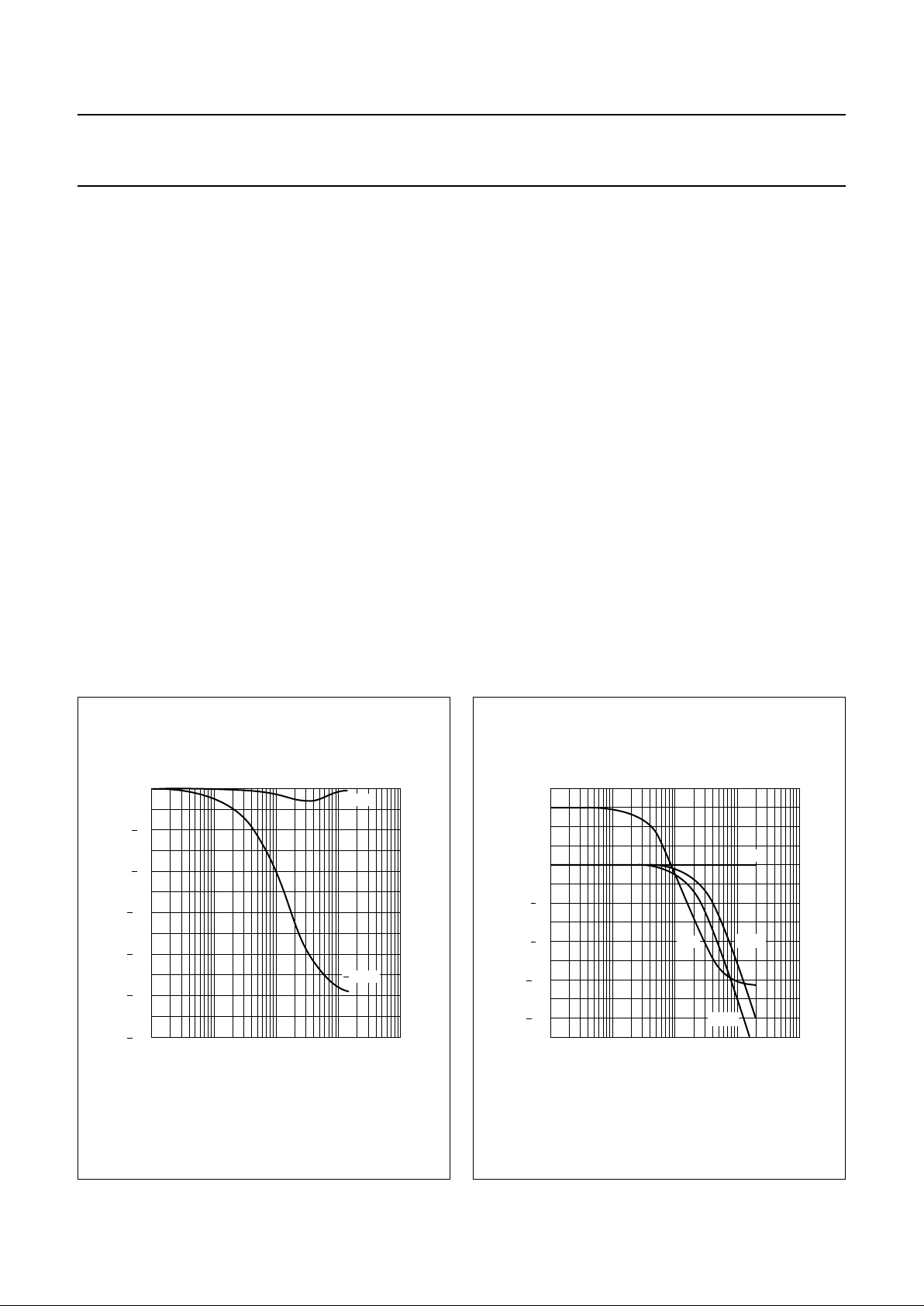
Noise Reduction (NR)
To improve the quality of the secondary channels, the
audio signal is processed at the transmitter side before
modulation. For an overall flat audio response the inverse
processing must take place after demodulation. This is
achieved in the NR.
The NR can be regarded as an input level dependent
Low-Pass Filter (LPF) [adaptive de-emphasis system]
followed by a fixed de-emphasis. Figure 3 shows the
transfer characteristics as function of the input level
(normalized to input level, and without the fixed
de-emphasis).
At maximum input level (50 kHz frequency deviation,
referred to as 0 dB) the frequency response of the first part
(i.e. without fixed de-emphasis) is nearly flat (note the
small dip around 3 kHz in Fig.3; this is a system attribute).
As the input level is X dB lowered, the higher output
frequencies will be reduced an extra X dB with respect to
the lower frequencies (1 : 2 expansion).
If a main carrier signal is received, the NR can be
bypassed at which the signal is fed directly to the
de-emphasis circuit. The noise reduction is active when
the NR signal (via I
2
C-bus) is logic 1.
De-emphasis
De-emphasis is realized by means of several internal
resistors and an external capacitor to ground. Via the
I
2
C-bus, the DEM signal can be switched between 50 µs,
75 µs, J17 and no de-emphasis. Figure 4 shows these
four different possibilities.
Output selection
With the output selector the output pins 23 and 22 can be
switched to the left and right satellite channels
(pins 33 and 31) or to the external inputs (pins 25 and 24)
for an other signal source or for connection of a decoder
box. the OS1 and OS0 bits determine this selection.
Pin 21 is a separate output which delivers the mono
channel. The mono signal is the sum of pin 23 (left) and
pin 22 (right) output signal [
1
⁄2(l + r)].
1996 Mar 11 10
Philips Semiconductors Preliminary specification
Satellite sound receiver with I2C-bus control
TDA8745
Output pins 23 and 22 can be muted by setting the
OML and OMR signals to logic 1. In addition, automatic
muting is also possible, the presence detector (as
described in Section “Presence detector”) sets the PDL bit
(PDR for other channel). Absence of a carrier at the
selected frequency results in automatic muting. This
mechanism is enabled or inhibited by the PDM bit
(Presence Detector auto Mute).
All outputs (pins 21, 22 and 23) are line drivers with
SCART level capability and are short-circuit protected by
means of 125 Ω output resistors. Pins 34 and 30 are also
line drivers at SCART level and can be used as signal
outputs before the IC’s output selection (i.e. for decoder
box use).
ABBREVIATIONS
BPF = Band-Pass Filter.
f
mod
= modulating frequency.
∆fM= frequency deviation of the main Channel.
∆fS1= frequency deviation of secondary Channel 1 (left).
∆fS2= frequency deviation of secondary Channel 2 (right).
f
OM
= carrier frequency of main Channel.
f
OS1
= carrier frequency of secondary Channel 1.
f
OS2
= carrier frequency of secondary Channel 2.
IF = Intermediate Frequency.
IL = Input Left.
IR = Input Right.
LPF = Low-Pass Filter.
NR = Noise Reduction.
OML = Output Mute Left.
OMR = Output Mute Right.
OS = Output Select.
PDM = Presence Detector auto Mute.
PE = Port Extension.
PLL = Phase-Locked Loop.
POR = Power-On Reset.
S/N = Signal-to-Noise ratio.
VCO = Voltage Controlled Oscillator.
handbook, halfpage
10
5
MBE284
10
4
10
3
10
2
10
4
0
8
12
16
20
24
transfer
(dB)
f (Hz)
20 dB
0 dB
Fig.4 Noise reduction transfer as function of
input level.
handbook, halfpage
10
5
MBE285
10
4
10
3
10
2
10
4
0
4
8
8
12
16
transfer
(dB)
f (Hz)
50 µs
75 µs
flat
J17
Fig.5 LF de-emphasis curves.

1996 Mar 11 11
Philips Semiconductors Preliminary specification
Satellite sound receiver with I2C-bus control
TDA8745
I2C-BUS PROTOCOL
Table 1 Slave receiver/transmitter address: D4 or D6 (HEX)
Notes
1. AS bit defined by level at address select (pin 12); 0 V = logic 0; 5 V = logic 1.
2. R/W = 0; TDA8745 is receiver (microcontroller is master transmitter).
R/W = 1; TDA8745 is transmitter (microcontroller is master receiver).
TDA8745 receiver use
In the receiver mode the device has four subaddresses with auto-increment, as shown in Tables 2 to 5.
Table 2 Input byte SA: 00; situation after POR
Table 3 Tuning byte SA: 01; situation after POR
Table 4 Select byte SA: 02; situation after POR
Table 5 Audio byte SA: 03; situation after POR
TDA8745 transmitter use
No subaddress.
Table 6 Read byte
BIT 7 BIT 6 BIT 5 BIT 4 BIT 3 BIT 2 BIT 1 BIT 0
110101AS
(1)
R/W
(2)
IL2
i7
IL1
i6
IL0
i5
IR2
i4
IR1
i3
IR0
i2
TUN9
i1
TUN8
i0
00000110
TUN7
t7
TUN6
t6
TUN5
t5
TUN4
t4
TUN3
t3
TUN2
t2
TUN1
t1
TUN0
t0
11101100
TEST
s7
BB
s6
OS1
s5
OS0
s4
PDM
s3
PE
s2
OML
s1
OMR
s0
00000011
LEV3
a7
LEV2
a6
LEV1
a5
LEV0
a4
NR
a3
DEM1
a2
DEM0
a1
BPFN
a0
11001110
PDL
r7
PDR
r6
−
r5
−
r4
−
r3
−
r2
−
r1
POR
r0
0 or 10 or 1111110 or 1

1996 Mar 11 12
Philips Semiconductors Preliminary specification
Satellite sound receiver with I2C-bus control
TDA8745
Slave receiver mode (bits transmitted from microcontroller to TDA8745)
Different IF inputs can be selected for the PLLs, for switching between different external BPFs and/or channels;
see Tables 7 and 8.
Table 7 IL2 to IL0; Input Left; note 1
Notes
1. X = don’t care.
2. Bit PE (s2) can be set to logic 1 to change IF input 5 into digital output for external switching purposes.
IL2
i7
IL1
i6
IL0
i5
PE
(2)
s2
MODE
0000IF input IN-1 selected for left PLL (after POR)
0010IF input IN-2 selected for left PLL
0100IF input IN-3 selected for left PLL
0110IF input IN-4 selected for left PLL
1000IF input IN-5 selected for left PLL
1010IF input IN-6 selected for left PLL
1100no selection
1110no selection
X 0 0 1 IF input IN-1 selected for left PLL
X 0 1 1 IF input IN-2 selected for left PLL
X 1 0 1 IF input IN-3 selected for left PLL
X 1 1 1 IF input IN-4 selected for left PLL
0 X X 1 IF input IN-5 used as output; 0 = 0 V
1 X X 1 IF input IN-5 used as output; 1 = 5 V
 Loading...