

Philips TDA8735, TDA8735T Datasheet

INTEGRATED CIRCUITS
DATA SH EET
TDA8735
PLL frequency synthesizer
Product specification
File under Integrated Circuits, IC01
Philips Semiconductors
September 1994
Philips Semiconductors Product specification
PLL frequency synthesizer TDA8735
FEATURES
• Complete 30 MHz single-chip tuning system
• Loop amplifier included
• 2-level current amplifier (charge pump) for adjusting the
loop gain
• A powerful digital memory phase detector
• Programmable reference frequencies of 1 kHz, 10 kHz
or 25 kHz
• I2C-bus interface
• Programmable address select input
• Software controlled switch output.
APPLICATIONS
• Satellite sound receiver
• Radio receiver: LW, MW and SW.
GENERAL DESCRIPTION
The TDA8735 is a single-chip PLL synthesizer designed
for satellite receivers. The device can be set to two
different addresses which can be used in applications
where independently tuned VCOs are required.
To adapt to different frequency accuracy, 3 reference
frequencies are selectable via the I2C-bus. The charge
pump current can be set to 2 values with a ratio of 1 : 100
via the I2C-bus.
A programmable switch (open collector) is integrated to
enable mode or normal switching, or other types of
application.
QUICK REFERENCE DATA
SYMBOL PARAMETER CONDITIONS MIN. TYP. MAX. UNIT
V
CC1
V
CC2
I
CC1
I
CC2
f
i(max)
f
i(min)
V
i(rms)
P
tot
T
amb
supply voltage (pin 3) 4.5 5.0 5.5 V
supply voltage (pin 16) V
CC1
8.5 12 V
supply current (pin 3) outputs unloaded 12 20 28 mA
supply current (pin 16) outputs unloaded 0.2 0.5 1 mA
maximum input frequency 30 −−MHz
minimum input frequency −−512 kHz
input voltage (RMS value) 30 − 500 mV
total power dissipation − 0.14 − W
operating ambient temperature −30 − +85 °C
ORDERING INFORMATION
TYPE
NUMBER
NAME DESCRIPTION VERSION
PACKAGE
TDA8735 DIP16 plastic dual in-line package; 16 leads (300 mil) SOT38-1
TDA8735T SO16 plastic small outline package; 16 leads; body width 3.9 mm SOT109-1
September 1994 2
Philips Semiconductors Product specification
PLL frequency synthesizer TDA8735
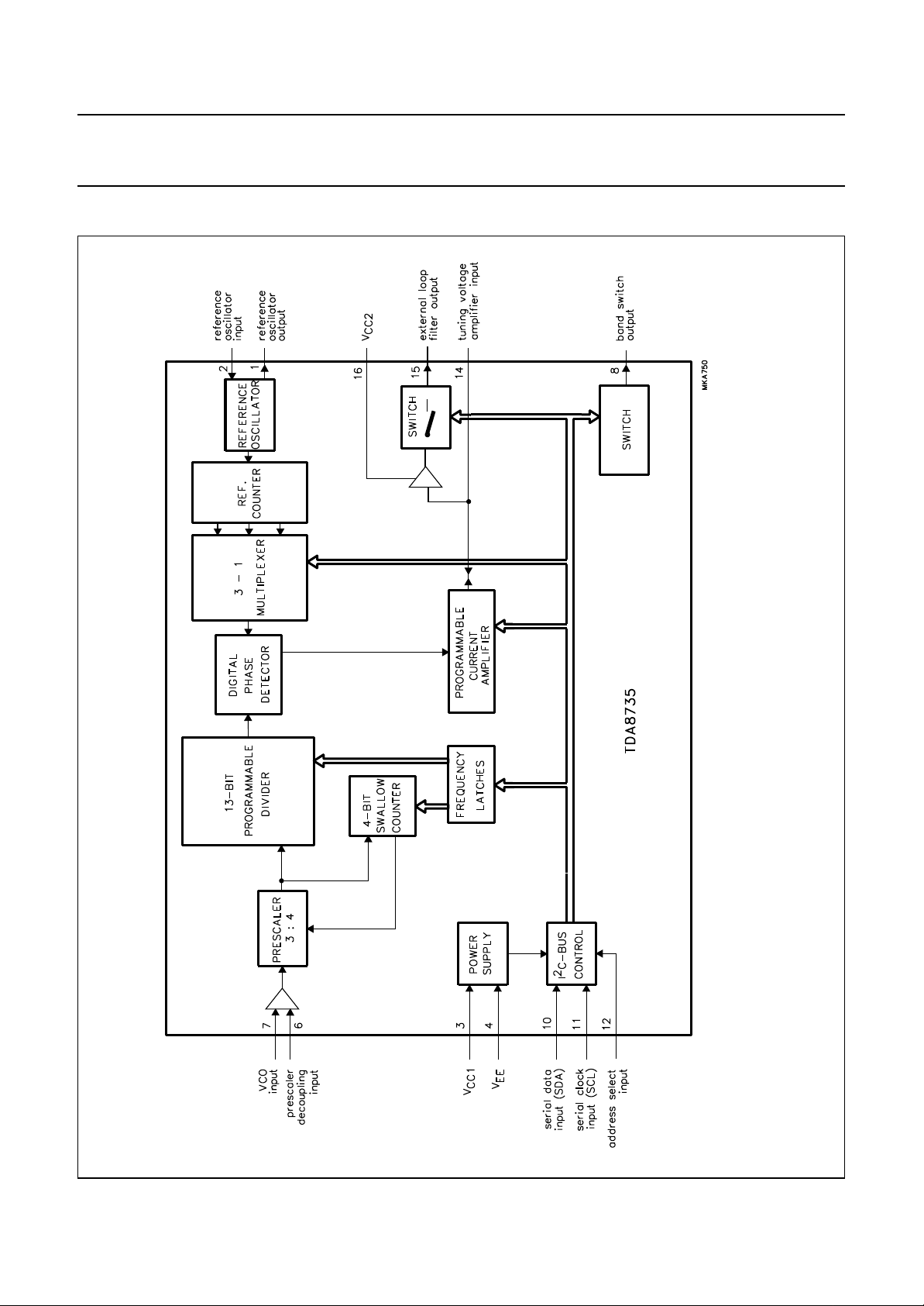
BLOCK DIAGRAM
September 1994 3
Fig.1 Block diagram.
Philips Semiconductors Product specification
PLL frequency synthesizer TDA8735
PINNING
SYMBOL PIN DESCRIPTION
XTAL1 1 reference oscillator output
XTAL2 2 reference oscillator input
V
CC1
V
EE
n.c. 5 not connected
DEC 6 prescaler decoupling
VCOFI 7 VCO input frequency
BS 8 band switch output
n.c. 9 not connected
SDA 10 serial data input (I
SCL 11 serial clock input (I
AS 12 address select input (I
n.c. 13 not connected
LOOP
I
LOOP
O
V
CC2
3 supply voltage 1
4 ground
2
C-bus)
2
C-bus)
2
C-bus)
14 tuning voltage amplifier input
15 external loop filter output
16 supply voltage 2
Fig.2 Pin configuration.
FUNCTIONAL DESCRIPTION
The TDA8735 contains the following parts and facilities:
• Input amplifier VCO-signal.
• A prescaler with the divisors 3 : 4 and a 2-bit
programmable swallow counter.
• A 13-bit programmable counter.
• A digital memory phase detector.
• A reference frequency channel comprised of a 4 MHz
crystal oscillator followed by a reference counter; the
reference frequency can be 1 kHz, 10 kHz or 25 kHz
and is applied to the digital memory phase detector.
2
C-bus interface with data latches and control logic;
• An I
the I2C-bus is intended for communication between
microcontrollers and different ICs or modules. Detailed
information on the I2C-bus specification is available on
request.
• A software-controlled switch output.
• A programmable current amplifier (charge pump) which
consists of a 5 µA and a 500 µA current source, this
allows adjustment of loop gain, thus providing
high-current high-speed tuning and low current-stable
tuning. The output at the loop amplifier can deliver a
tuning voltage of up to 10.5 V (V
CC2
− 1.5 V).
Controls
The TDA8735 is controlled via the 2-wire I
2
C-bus. As slave
receiver for programming there is one module address, a
logic 0 (R/W bit), a subaddress byte and four data bytes.
The subaddress determines which one of the four data
bytes is transmitted first. The module address contains a
programmable address bit (D1) which with address select
input AS (pin 12) makes it possible to operate two
TDA8735 in one system.
The auto increment facility of the I2C-bus allows
programming of the TDA8735 within one transmission
(address + subaddress + 4 data bytes).
The TDA8735 can also be partially programmed.
Transmission must then be ended by a stop condition.
The bit organization of the 4 data bytes is illustrated in
Fig.3 and is described below.
The divider number is defined by 15-bit words, bits
S0 to S14. To calculate the lock frequency, the divider
number has to be multiplied by the selected reference
frequency.
September 1994 4
Philips Semiconductors Product specification
PLL frequency synthesizer TDA8735
Table 1 Divider number setting.
ON DIVIDER NUMBER SETTING INPUT
1
0 (S0 + S1) × 2
Where the minimum divider ratio is: 2
.... + S13 × 213+ S14 × 2
6
=64to215− 1 = 32761.
Table 2 Bit CP (used to control the charge pump;
DB0: D0).
CP CURRENT
0 LOW
1 HIGH
Table 3 Bits REF1 and REF2 (used to set the reference
frequency applied to the phase detector;
DB2: D7 and D6).
14
ON
REF1 REF2
FREQUENCY
(kHz)
00 1
01 10
10 25
11 0
Table 4 Bit OPAMP (used to control the switch in the
tuning voltage amplifier output circuitry;
DB2: D4).
OPAMP SWITCH
1on
0off
Table 5 Bit BS (used to control the open-collector switch
output; DB2: D2).
BS SWITCH OUTPUT
1 sink current
0 floating
The data byte DB3 must be set to 0....0. It is also used for
test purposes (see Fig.3).
September 1994 5
 Loading...