

Philips TDA8732 Datasheet

INTEGRATED CIRCUITS
DATA SH EET
TDA8732
NICAM-728 demodulator (NIDEM)
Product specification
File under Integrated Circuits, IC02
April 1993
Philips Semiconductors Product specification
NICAM-728 demodulator (NIDEM) TDA8732
FEATURES
• 5 V supplies for analog and digital circuitry
• Low cost application
• Improved noise behaviour
• Limiting amplifier for QPSK input
• Suitable with PAL B, G and I NICAM-728 systems.
GENERAL DESCRIPTION
The NIDEM is a dedicated device providing a DQPSK
(Differential Quadrature Phase Shift Keying) demodulator
for a NICAM-728 system.
The device interfaces with NICAM-728 decoders and
provides data synchronized to a 728 kHz clock (either
supplied externally or by the on-board clock).
The device consists of a costas loop quadrature
demodulator, a bit-rate clock recovery and differential
APPLICATIONS
• NICAM-728 systems.
decoder with parallel-to-serial conversion.
The Voltage Controlled Oscillator (VCO) used in the
costas loop is achieved with a single-pin crystal oscillator.
A second single-pin crystal oscillator with a divider chain
provides signals at 5.824 MHz and at 728 kHz.
The NIDEM is suitable for PAL B and G (carrier oscillator
crystal at 11.7 MHz) and PAL I (carrier oscillator crystal at
13.104 MHz).
QUICK REFERENCE DATA
Measured over full voltage and temperature ranges.
SYMBOL PARAMETER MIN. TYP. MAX. UNIT
V
CCA
V
CCD
V
CCA
V
CCA−VCCD
I
CCA
I
CCD
V
3
R
I
C
I
f
CAROSC
f
XTAL
analog supply voltage 4.5 5 5.5 V
digital supply voltage 4.5 5 5.5 V
analog supply voltage 4.5 5 5.5 V
differential supply voltage −0.5 − 0.5 V
analog supply current − 12.5 − mA
digital supply current − 14.5 − mA
QPSK input level (peak-to-peak value) 30 100 300 mV
input resistance 1.75 2.5 3.25 kΩ
input capacitance − 2 − pF
carrier oscillator frequency 11.5 − 13.5 MHz
crystal frequency
PAL B, G − 11.7 − MHz
PAL I − 13.104 − MHz
f
CLKOSC
clock oscillator frequency − 11.648 − MHz
f
C5M
C5M output frequency − 5.824 − MHz
ORDERING INFORMATION
EXTENDED
PACKAGE
TYPE
NUMBER
PINS PIN POSITION MATERIAL CODE
TDA8732 20 DIL plastic SOT146
Note
1. SOT146-1; 1996 December 3.
April 1993 2
(1)
Philips Semiconductors Product specification
NICAM-728 demodulator (NIDEM) TDA8732
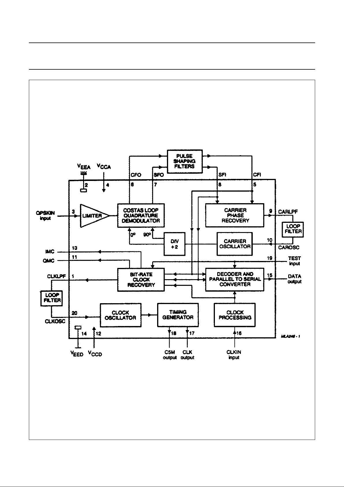
Fig.1 Block diagram.
April 1993 3
Philips Semiconductors Product specification
NICAM-728 demodulator (NIDEM) TDA8732
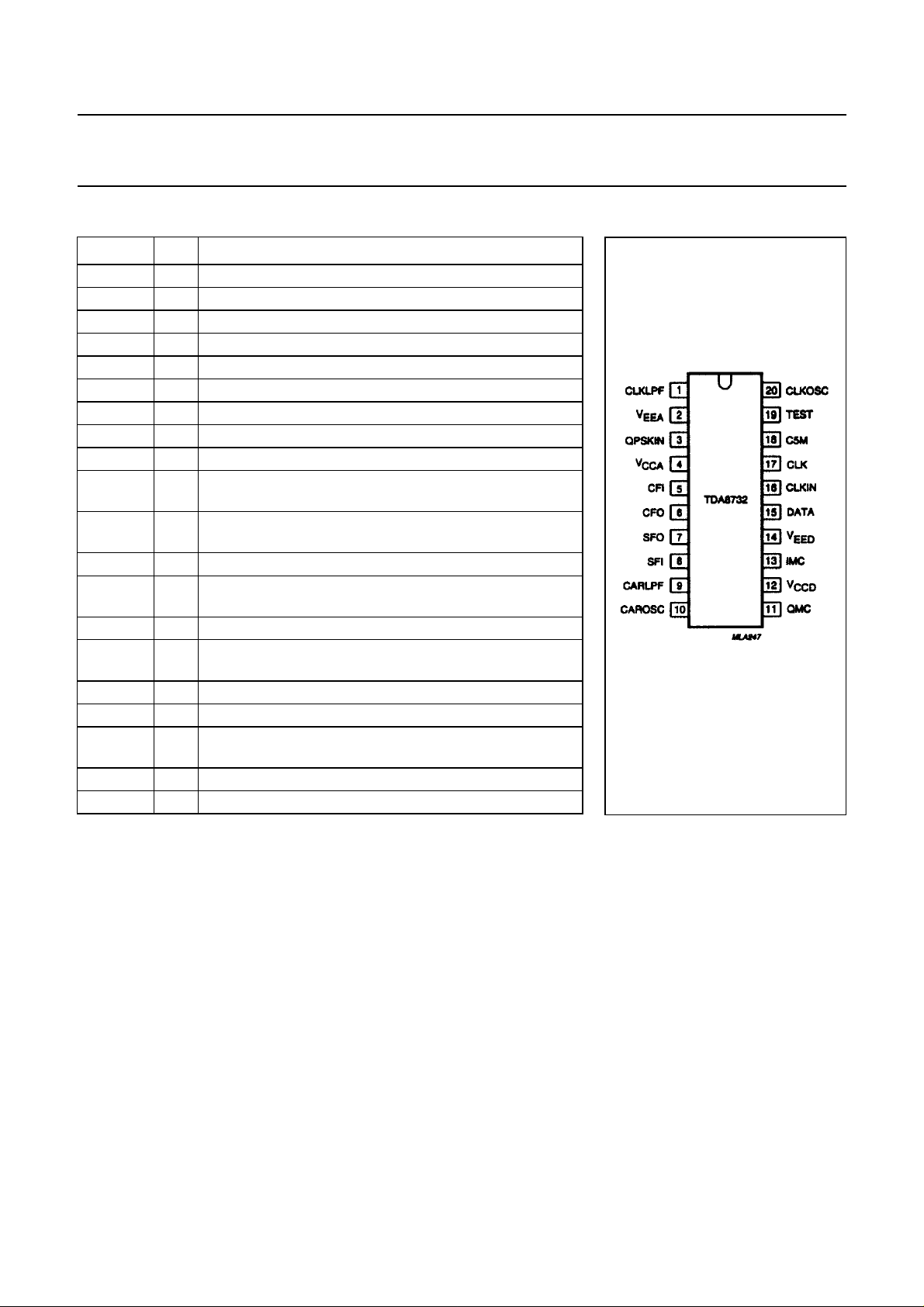
PINNING
SYMBOL PIN DESCRIPTION
CLKLPF 1 transconductance output for bit-rate loop low-pass filter
V
EEA
QPSKIN 3 QPSK modulated data input
V
CCA
CFI 5 baseband cosine channel input after filtering
CFO 6 demodulated cosine channel output to low-pass filter
SFO 7 demodulated sine channel output to low-pass filter
SFI 8 baseband sine channel input after filtering
CARLPF 9 transconductance output for carrier loop low-pass filter
CAROSC 10 crystal input for carrier oscillator (frequency is 11.7 MHz
QMC 11 monostable components connection for quadrature data
V
CCD
IMC 13 monostable components connection for in-phase data
V
EED
DATA 15 728 kbit/s demodulated and differentially decoded serial
CLKIN 16 bit-rate clock input at 728 kHz, phase-locked to the data
CLK 17 output clock frequency at 728 kHz
C5M 18 reference frequency output at
TEST 19 input for test purpose (grounded for normal operation)
CLKOS 20 crystal input for clock oscillator (frequency is 11.648 MHz)
2 ground for analog circuitry
4 power supply for analog circuitry
or 13.104 MHz)
transition detector
12 power supply for digital circuitry
transition detector
14 ground for digital circuitry
data output
5.824 MHz (8 x CLK)
Fig.2 Pin configuration.
April 1993 4

Philips Semiconductors Product specification
NICAM-728 demodulator (NIDEM) TDA8732
FUNCTIONAL DESCRIPTION
QPSK demodulator
The DQPSK signal input to the demodulator (QPSKIN) is
limited and fed into the costas loop demodulator. A
single-pin carrier oscillator (CAROSC), at twice the carrier
frequency, supplies a differential signal to the divider
circuitry, which drives the demodulators with both 0° and
90° phase shift. This produces cosine and sine signals
which are required for the carrier recovery. Cosine
(in-phase) and sine (in Quadrature) channel baseband
filters are then provided externally between pins CFO and
CFI, and SFO and SFI respectively. The two filtered
baseband signals are then processed to provide an error
signal, the magnitude and which of which bear a fixed
relationship to the phase error of the carrier, regardless of
which of the four rest-states the signal occupies. The
carrier recovery loop is closed with the aid of a single pin
loop filter connection at CARLPF, which filters the error
voltage signal to control the 728 kHz as shown in
application diagrams Fig.4 and 5.
Bit-rate clock recovery loop
The CFI and SFI channels are processed using edge
detectors and monostables, with externally derived time
constants (see Fig.3), to generate a signal with a coherent
component at the data bit symbol rate. This signal is
compared with the clock derived from CLKIN and used to
produce an error signal at the transconductance output
CLKLPF. This error signal is loop-filtered and used to
control the clock generator (at CLKOSC if the on-board
clock is used; see Fig.5).
Clock oscillator and timing generator
A voltage-controlled oscillator on-board the NIDEM
operates at 11.648 MHz and is divided down to produce a
728 kHz (bit-rate) clock output (CLK) which is phase
locked to the pulse stream and may be used as an
alternative clock input for NIDEM. A reference clock at
5.824 MHz is provided at pin C5M (TTL levels).
Differential decoder and parallel-to-serial converter
The recovered symbol-rate clocking-signal (364 kHz)
produced internally is passed to the demodulator where it
samples the sliced raised cosine pulse stream. The
recovered bit-rate clocking-signal is passed to the decoder
and is used to differentially decode the demodulated data
signal and reform it into a serial bit-stream.
April 1993 5
 Loading...