

Philips TDA8730 Datasheet

INTEGRATED CIRCUITS
DATA SH EET
TDA8730
PLL FM demodulator for DBS
signals
Preliminary specification
File under Integrated Circuits, IC02
March 1991

Philips Semiconductors Preliminary specification
PLL FM demodulator for DBS signals TDA8730
FEATURES
• Broadband IF amplifier
• PLL demodulator, consisting of:
– a multiplier
– a voltage controlled oscillator
– a loop amplifier
GENERAL DESCRIPTION
The TDA8730 is a sensitive PLL
demodulator for the second IF and
direct broadcasting satellite (DBS)
receivers. It provides AGC output and
threshold adjustment for optimal signal
level at the input of the demodulator.
• AGC detector and DC amplifier
• LOW impedance video and data output
• Power supply voltage stabilizer
QUICK REFERENCE DATA
SYMBOL PARAMETER CONDITIONS MIN. TYP. MAX. UNIT
V
I
V
f
f
V
V
DD
DD
I
osc
osc
O
AGC
supply voltage − 9 − V
supply current − 75 − mA
input voltage level − 70 − dBµV
minimum oscillator frequency − 130 − MHz
maximum oscillator frequency − 720 − MHz
video output signal amplitude (peak-to-peak
value)
AGC output voltage 1.8 − V
note 1 − 1.1 − V
DD
V
Note
1. ∆f = 13.5 MHz (peak-to-peak value)
ORDERING AND PACKAGE INFORMATION
EXTENDED TYPE
NUMBER
PINS PIN POSITION MATERIAL CODE
PACKAGE
TDA8730 16 DIL plastic SOT38GE
Note
1. SOT38-1; 1996 December 4.
(1)
March 1991 2
Philips Semiconductors Preliminary specification
PLL FM demodulator for DBS signals TDA8730
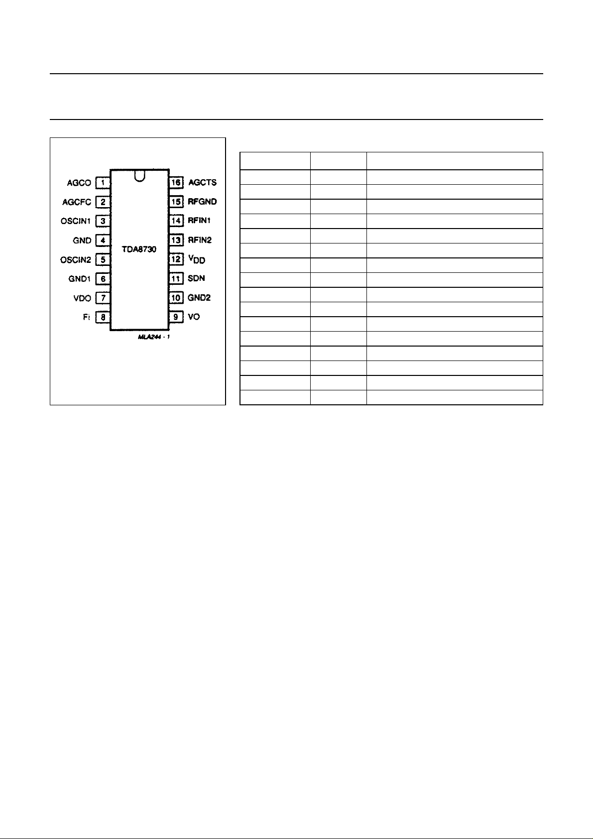
PINNING
SYMBOL PIN DESCRIPTION
AGCO 1 AGC output
AGCFC 2 AGC frequency compensation
OSCIN1 3 oscillator input 1
GND 4 GND
OSCIN2 5 oscillator input 2
GND1 6 ground 1
VDO 7 variable capacitor drive output
FI 8 feedback input
VO 9 video output
GND2 10 ground 2
SDN 11 stabilizer decoupling node
Fig.1 Pinning diagram.
V
DD
RFIN2 13 RF input 2
RFIN1 14 RF input 1
RFGND 15 RF ground
AGCTS 16 AGC threshold setting
12 supply voltage +9V
APPLICATIONS
Direct broadcasting satellite (DBS) receivers.
March 1991 3
 Loading...