

Philips TDA8722T-C2, TDA8722T-C3, TDA8722T-C1, TDA8722M-C2, TDA8722M-C3 Datasheet
...
DATA SH EET
Product specification
Supersedes data of 1995 Mar 21
File under Integrated Circuits, IC02
1998 Jun 23
INTEGRATED CIRCUITS
TDA8722
I
2
C-bus programmable modulator
for negative video modulation and
FM sound

1998 Jun 23 2
Philips Semiconductors Product specification
I2C-bus programmable modulator for
negative video modulation and FM sound
TDA8722
FEATURES
• Video amplifier with clamp and white clip circuits
• FM sound modulator
• Asymmetrical and symmetrical RF outputs available
• Symmetrical RF oscillator using only a few external
components
• External adjusting of modulation depth and level of the
sound subcarrier
• I2C-bus receiver for frequency setting and test-mode
selection
• One I
2
C programmable output port
• On-chip Phase-Locked Loop (PLL) frequency
synthesizer
• On-chip power supply regulator
• Bus switchable oscillator
• On-chip Test Pattern Signal Generator (TPSG).
APPLICATIONS
• Video recorders
• Cable converters
• Satellite receivers.
GENERAL DESCRIPTION
The TDA8722 is a programmable modulator which
generates an RF TV channel from a baseband video
signal and a baseband audio signal in the event of
negative video and FM sound standards (PAL B/G, I, D/K
and NTSC).
It is especially suited for satellite receivers, video
recorders and cable converters. The video carrier
frequency is set exactly to the correct channel frequency
by a PLL synthesizer which is programmed in accordance
with the I2C-bus format.
ORDERING INFORMATION
TYPE
NUMBER
PACKAGE
NAME DESCRIPTION VERSION
TDA8722T SO20 plastic small outline package; 20 leads; body width 7.5 mm SOT163-1
TDA8722M SSOP20 plastic shrink small outline package; 20 leads; body width 4.4 mm SOT266-1

1998 Jun 23 3
Philips Semiconductors Product specification
I2C-bus programmable modulator for
negative video modulation and FM sound
TDA8722
QUICK REFERENCE DATA
V
DDA=VDDD
=5V; T
amb
=25°C after the IC has reached thermal equilibrium; unless otherwise specified.
Notes
1. Value depends on value of resistor R17 (see Fig.7).
2. Value depends on value of capacitor C17 (see Fig.7).
SYMBOL PARAMETER CONDITIONS MIN. TYP. MAX. UNIT
V
DDA
analog supply voltage 4.5 5.0 5.5 V
V
DDD
digital supply voltage 4.5 5.0 5.5 V
I
DD
total supply current normal mode 41 52 63 mA
∆m typical modulation depth range video level (pin 19) = 0.5 V (p-p);
note 1; see Fig.10
65 − 90 %
∆P/S typical picture-to-sound level
range
note 2; see Fig.11 −18 −−10 dB
V
RF
RF output voltage level
asymmetrical on a 75 Ω load
frequency between
471.25 and 855.25 MHz
77 80 83 dBµV
δf FM deviation on audio
subcarrier
f
i
= 400 Hz; V1= 0.5 V (RMS);
before pre-emphasis filter
20 25 30 kHz
1998 Jun 23 4
Philips Semiconductors Product specification
I2C-bus programmable modulator for
negative video modulation and FM sound
TDA8722
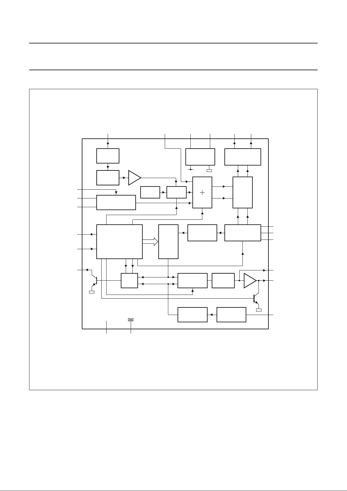
BLOCK DIAGRAM
Fig.1 Block diagram.
handbook, full pagewidth
MBE401
LOGIC
enable/
select
f
DIV
f
ref
14
10 bits
I C-BUS
2
RECEIVER
12-BIT
DIVIDER
(N)
PHASE
DETECTOR
enable
CHARGE
PUMP
AMP
7
DIVIDER
(M = 128)
31.25 kHz
4 MHz
OSCILLATOR
9
XTAL
11
V
DDD DGND
10
8
AMP
CP
PRESCALER
(8)
ASYMMETRICAL
OUTPUT
BUFFER
UHF
OSCILLATOR
TDA8722
4
5
6
UOSCB
OGND
UOSCA
RF oscillator on
PC
AUDIO
FM MODULATOR
12
13
SDA
SCL
P0
SOSCB
SOSCA
AUDIO
3
2
1
SWITCH
TPSG
balance test
TPSG on
MIXER
16 15
VOLTAGE
REGULATOR
18 2017
ADJUST AGNDVDDA
RFA RFB
CLIP
CLAMP
19
VIDEO
VIDEO AMP
1998 Jun 23 5
Philips Semiconductors Product specification
I2C-bus programmable modulator for
negative video modulation and FM sound
TDA8722
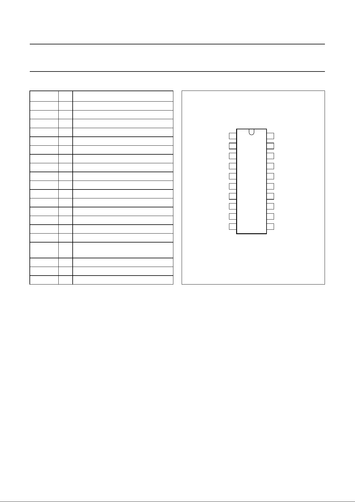
PINNING
SYMBOL PIN DESCRIPTION
AUDIO 1 audio input
SOSCA 2 sound oscillator A
SOSCB 3 sound oscillator B
UOSCB 4 UHF oscillator B
OGND 5 RF oscillator ground
UOSCA 6 UHF oscillator A
AMP 7 tuning amplifier output
CP 8 charge pump output
XTAL 9 crystal oscillator
DGND 10 digital ground
V
DDD
11 digital supply voltage
SCL 12 serial clock input (I
2
C-bus)
SDA 13 serial data input (I
2
C-bus)
P0 14 NPN open-collector output Port
RFB 15 asymmetrical RF output B
RFA 16 asymmetrical RF output A
ADJUST 17 modulation depth and picture-to-sound
distance adjustment pin
AGND 18 analog ground
VIDEO 19 video input
V
DDA
20 analog supply voltage
Fig.2 Pin configuration.
handbook, halfpage
TDA8722
MBE394
1
2
3
4
5
6
7
8
9
10
20
19
18
17
16
15
14
13
12
11
CP
DGND
XTAL SCL
SDA
AMP P0
UOSCA RFB
OGND RFA
UOSCB ADJUST
SOSCB AGND
SOSCA VIDEO
AUDIO
V
DDD
V
DDA
FUNCTIONAL DESCRIPTION
The TDA8722 is a programmable modulator which can be
divided into two main blocks:
• A modulator for negative video modulation and
FM sound TV standards
• A programmable PLL frequency synthesizer.
The video part of the modulator consists of a clamping
circuit which sets the internal reference voltage to the
bottom of the synchronizing pulse, followed by a white clip
which avoids over modulation in case the video signal is
too strong. Typically, the IC starts to clip the video signal
when the voltage at the video input (pin 19) is
>560 mV (p-p) while the normal voltage at the video input
is 500 mV (p-p). This clipping function ensures that the
video modulation depth is not too high. The modulation
depth is adjusted in the application between at least
65 and 90% by changing the resistor value between pin 17
and ground (R17). The value can change between 47 kΩ
and infinite (R17 removed); see Fig.10.
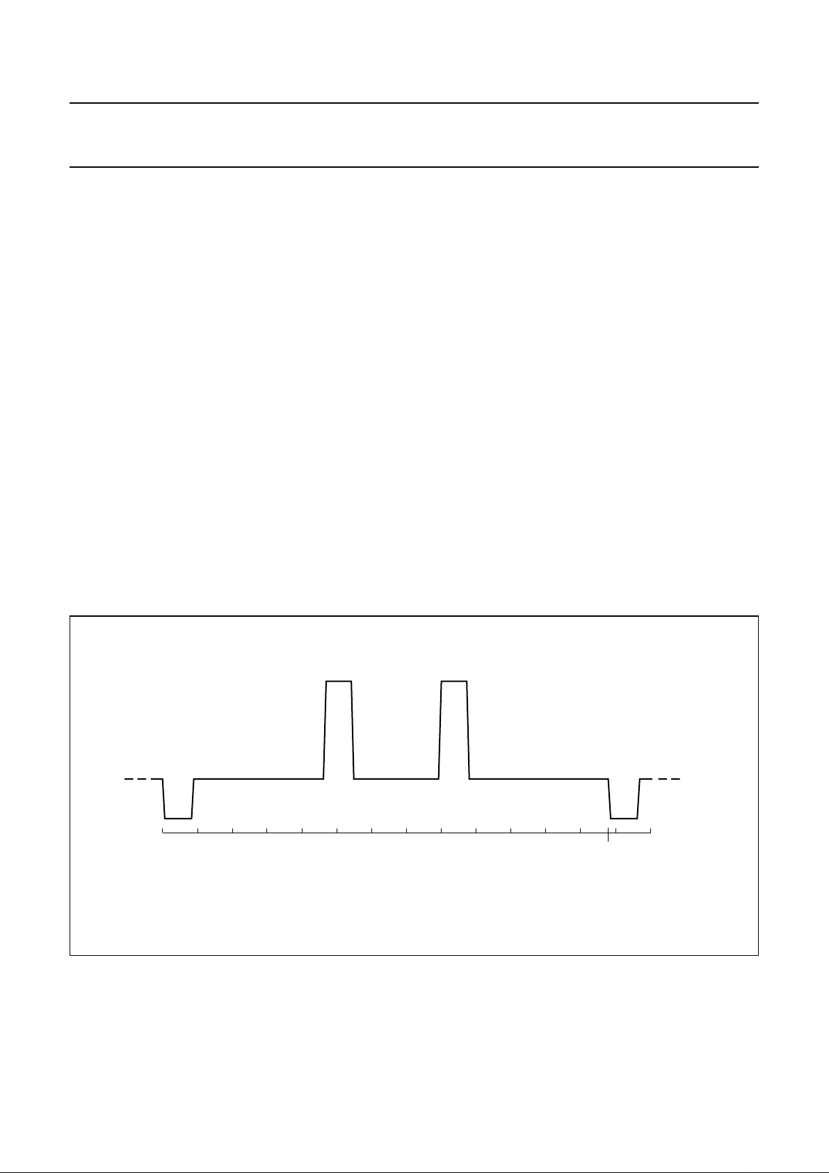
The video part also contains a test pattern signal generator
to simplify the adjustment of the receiving channel of the
TV set to the required channel of the modulator. The
pattern consists of a synchronization pulse and two
vertical white bars on screen (see Fig.3).
The audio part of the modulator contains an FM sound
modulator. The frequency of the sound subcarrier is set in
the application by external components (C3, L3 and R3).
The difference between the video carrier level and the
sound subcarrier level is adjusted in the application by
changing the value of the capacitor between pin 17 and
ground (C17). The value can change between
0 and 47 pF. The distance between the video carrier and
the sound subcarrier can be adjusted between at least
−10 and −18 dB (see Fig.11).
1998 Jun 23 6
Philips Semiconductors Product specification
I2C-bus programmable modulator for
negative video modulation and FM sound
TDA8722
To bias the audio input it is necessary to put a resistor in
the application between pin 1 and ground. The resistor
has a typical value of 12 kΩ.
The RF part of the oscillator consists of:
• An oscillator which operates at the required video
carrier frequency. The range of the oscillator is
determined in the application by C5, C6, L5 and D5.
• An RF mixer. It first combines the video signal and the
sound subcarrier to build a baseband TV channel.
Then the baseband signal is mixed with the oscillator
signal to get the RF TV channel. The mixer has two
outputs which can be used as two independent
asymmetrical outputs, or as one symmetrical output. In
the event of asymmetrical use, the unused output must
be loaded with a 75 Ω resistor (see Fig.7).
The oscillator frequency is set by a programmable PLL
frequency synthesizer in accordance with equation:
f
osc
=8×N×f
ref
Where:
f
osc
is the local oscillator frequency.
N is a 12-bit dividing number (10 bits are programmable
by the I2C-bus).
f
ref
is the crystal frequency (4 MHz) divided by 128
(31.25 kHz).
The circuit allows a step of 250 kHz but because only
10 bits are programmable, the programming steps are
1 MHz.
When the PLL loop is locked, both inputs of the phase
comparator are equal, which gives equation:
During the test mode operation, f
DIV
and f
ref
can be
monitored on the output Port pin (pin 14).
Software information
The synthesizer is controlled via a two-wire I
2
C-bus
receiver. For programming, the address byte (C8 HEX)
has to be sent first. Then one or two data bytes are used
to set the 10 programmable bits of the dividing number N,
the test bits (see Table 1) and the output Port state. Note
that after power-up of the IC, the two data bytes must be
sent.
f
DIV
f
osc
8N×
-------------
f
xtal
128
--------- -
f
ref
===
Fig.3 Test pattern signal.
handbook, full pagewidth
010203040 50 60
64
70
MBE395
t (µs)

1998 Jun 23 7
Philips Semiconductors Product specification
I2C-bus programmable modulator for
negative video modulation and FM sound
TDA8722
Table 1 Data format; notes 1 and 2
Notes
1. The 10 programmable bits of N are: b2 to b11.
2. Internal hardware sets: b1 = 0 and b0 = 1.
3. T0, T1 and T2 are bits used for test purposes (see Table 5).
4. P0 is a bit used for controlling the state of the output Port (see Table 6).
Table 2 Structure of the dividing number N
Notes
1. Bits b2 to b11 are programmable and represent the integer part of the frequency in MHz. Bits b1 and b0 are fixed
internally to b1 = 0 and b0 = 1 to get the added 0.25 MHz, common for most TV channels.
2. Bits b1 and b0 are not programmable.
3. f
osc
= 512b11 + 256b10 + 128b9 + 64b8 + 32b7 + 16b6 + 8b5 + 4b4 + 2b3 + b2 + 0.25 (MHz).
Table 3 Dividing number N for programming channel 21 (471.25 MHz)
Notes
1. Bits b1 and b0 are not programmable.
2. f
osc
=0+256+128+64+0+16+0+4+2+1+0.25 (MHz) = 471.25 MHz.
Table 4 Content of the data bytes to program channel 21 (471.25 MHz)
It is possible to change only one data byte. The circuit will recognize which one is received with the value of MSB
(0 for data byte 1 and 1 for data byte 2). It is possible to change the frequency by 1 MHz with data byte 2. It is easy to
increment the channel frequency when its frequency width is 8 MHz by simply incrementing data byte 1.
BYTE
BIT 7
MSB
BIT 6 BIT 5 BIT 4 BIT 3 BIT 2 BIT 1
BIT 0
LSB
ACKNOWLEDGE BIT
Address byte C8 1 1 0 0 1 0 0 0 ACK
Data byte 1 0 b11 b10 b9 b8 b7 b6 b5 ACK
Data byte 2 1 T0
(3)
T1
(3)
T2
(3)
P0
(4)
b4 b3 b2 ACK
RESULT
BITS
(1)
b11 b10 b9 b8 b7 b6 b5 b4 b3 b2 b1
(2)
b0
(2)
Frequency (MHz)
(3)
51225612864321684210.50.25
RESULT
BITS
b11 b10 b9 b8 b7 b6 b5 b4 b3 b2 b1
(1)
b0
(1)
Value 011101011101
Frequency (MHz)
(2)
025612864016042100.25
BYTE
BIT 7
MSB
BIT 6 BIT 5 BIT 4 BIT 3 BIT 2 BIT 1
BIT 0
LSB
ACKNOWLEDGE BIT
Address byte C8 1 1 0 0 1 0 0 0 ACK
Data byte 1 0 0 1 1 1 0 1 0 ACK
Data byte 2 1 0 0 0 0 1 1 1 ACK
1998 Jun 23 8
Philips Semiconductors Product specification
I2C-bus programmable modulator for
negative video modulation and FM sound
TDA8722
The bits T0 to T2 are available for test purposes and the possibilities are shown in Table 5.
Table 5 Test modes
Notes
1. In ‘TPSG on’ mode the video carrier is modulated by the test signal consisting of a synchronization pulse and two
vertical white bars on a black screen. This mode should be selected to adjust the TV set receiving the modulated
signal to the right frequency.
2. In ‘RF oscillator off’ mode, the RF oscillator and the RF mixer are switched-off and there is no RF carrier coming out
of the device. This mode can be selected to avoid RF radiation to other parts when the modulator output is not used.
3. In ‘balance test’, the video carrier is over modulated. This simplifies residual carrier measurements.
4. In ‘f
ref
’ and ‘f
DIV
’ modes, the reference frequency f
ref
in the phase comparator or the divided RF oscillator frequency
f
DIV
is available on the output Port pin. This mode requires that bit P0 = 0.
5. The ‘high-impedance test’ mode may be used to inject an external tuning voltage to the RF tank circuit, to test the
oscillator. In this mode, the phase detector is disabled and the external transistor of the tuning amplifier is
switched-off. The AMP output (pin 7) is LOW (<200 mV).
6. In the ‘phase detector disabled’ mode, it is possible to measure the leakage current at the input of the tuning amplifier,
on the CP pin. In this mode the RF oscillator is off, and the baseband TV channel signal is present on the RF outputs
for testing the audio and video parts.
T0 T1 T2 OPERATIONAL MODE
0 0 0 normal operation
0 0 1 Test Pattern Signal Generator (TPSG) on; note 1
0 1 0 RF oscillator off; note 2
0 1 1 balance test; note 3
100f
ref
out (if p0 = 0); note 4
1 0 1 high-impedance test; note 5
110f
DIV
out (if p0 = 0); note 4
1 1 1 phase detector disabled; baseband signals on RF outputs; note 6
The possibilities of bit P0, which controls the output Port
(pin 14) are given in Table 6.
The Port is an NPN open-collector type. For monitoring the
f
ref
or f
DIV
frequency on the output Port, the P0 bit must be
logic 0 to let the output Port free.
Table 6 Output Port programming
P0 OUTPUT PORT STATE
0 off; high impedance
1 on; sinking current

1998 Jun 23 9
Philips Semiconductors Product specification
I2C-bus programmable modulator for
negative video modulation and FM sound
TDA8722
LIMITING VALUES
In accordance with the Absolute Maximum Rating System (IEC 134).
HANDLING
Inputs and outputs are protected against electrostatic discharge in normal handling. However, to be completely safe, it
is desirable to take normal precautions appropriate to handling integrated circuits. Every pin withstands the ESD test in
accordance with
“MIL-STD-883C category B”
(2000 V). Every pin withstands the ESD test in accordance with Philips
Semiconductors Machine Model (MM) 0 Ω, 200 pF (200 V).
THERMAL RESISTANCE
SYMBOL PARAMETER MIN. MAX. UNIT
V
DDA
analog supply voltage −0.3 +6 V
V
DDD
digital supply voltage −0.3 +6 V
V
DD
operating supply voltage 4.5 5.5 V
V
max
maximum voltage on all pins −0.3 V
DD
V
T
stg
IC storage temperature −40 +125 °C
T
amb
operating ambient temperature −20 +85 °C
SYMBOL PARAMETER VALUE UNIT
R
th j-a
thermal resistance from junction to ambient in free air
SO20; SOT163-1 85 K/W
SSOP20; SOT266-1 120 K/W
 Loading...