

Philips TDA8718X-C1, TDA8718K-C1-R1, TDA8718K-C1 Datasheet

DATA SH EET
Product specification
Supersedes data of April 1993
File under Integrated Circuits, IC02
June 1994
INTEGRATED CIRCUITS
Philips Semiconductors
TDA8718
8-bit high-speed analog-to-digital
converter

June 1994 2
Philips Semiconductors Product specification
8-bit high-speed analog-to-digital converter TDA8718
FEATURES
• 8-bit resolution
• Sampling rate up to 600 MHz
• ECL (100K family) compatible for digital inputs and
outputs
• Overflow/Underflow output
• 50 Ω load drive capability
• Low input capacitance (5 pF typ.).
APPLICATIONS
• High speed analog-to-digital conversion
• Industrial instrumentation
• Data communication
• RF communication.
GENERAL DESCRIPTION
The TDA8718 is an 8-bit analog-to-digital converter (ADC)
designed for professional applications. The device
converts the analog input signal into 8-bit binary coded
digital words at a sampling rate of 600 MHz. It has an
effective bandwidth capability up to 150 MHz full-scale
sine wave. All digital outputs are ECL compatible.
QUICK REFERENCE DATA
Measured over full voltage and temperature ranges, unless otherwise specified.
ORDERING INFORMATION
SYMBOL PARAMETER CONDITIONS MIN. TYP. MAX. UNIT
V
EEA
analog supply voltage −4.2 −4.5 −4.8 V
V
EED
digital supply voltage −4.2 −4.5 −4.8 V
I
ref
resistive ladder current R = 48 Ω 30 45 60 mA
I
EEA
analog supply current 30 42 54 mA
I
EED
digital supply current 100 120 150 mA
I
EEO(L)
LOW level output supply current RL = 50 Ω 40 70 90 mA
I
EEO(H)
HIGH level output supply current RL = 50 Ω 155 170 185 mA
ILE DC integral linearity error −±0.7 ±1.0 LSB
DLE DC differential linearity error −±0.3 ±0.5 LSB
EB effective bits f
i
= 4.43 MHz; I
ref
= 45 mA;
f
clk
= 100 MHz
− 7.5 − bits
f
i
= 4.43 MHz; I
ref
= 45 mA;
f
clk
= 100 MHz
− 6.5 − bits
f
clk(max)
maximum clock frequency 600 −−MHz
P
tot
total power dissipation − 990 1250 mW
TYPE NUMBER
PACKAGE
PINS PIN POSITION MATERIAL CODE
TDA8718K 28 PLCC28 plastic SOT261-2

June 1994 3
Philips Semiconductors Product specification
8-bit high-speed analog-to-digital converter TDA8718
BLOCK DIAGRAM
Fig.1 Block diagram.
handbook, full pagewidth
1
3
5
V
RB
V
I
21
2389
CLK CLK
V
EED
28
V
EEA
16
15
13
17 D2
D3
D4
D5
D6
19
20
10
D1
D0
D7
ECL OUTPUTS
CLOCK DRIVER
TDA8718
analog
voltage input
clock inputs
underflow
output
data outputs
LSB
MSB
14
ANALOG SIGNAL
PROCESSING
RESISTOR
LADDER
&
INPUT
AND
OUTPUT
LATCHES
&
DIGITAL
DECODING
MBB854 - 2
24
DGND
27
AGND
analog ground digital ground
V
BB
UF
OGND2
OF
overflow
output
output
ground
analog negative
supply voltage
digital negative
supply voltage
32
8
8
V
RT
VRM2
reference
voltage middle
reference
voltage TOP
reference
voltage BOTTOM
11
6
18
Ω
Ω
Ω
12
OGND1

June 1994 4
Philips Semiconductors Product specification
8-bit high-speed analog-to-digital converter TDA8718
PINNING
SYMB
OL
PIN DESCRIPTION
V
RB
1 reference voltage BOTTOM
V
RM
2 reference voltage MIDDLE decoupling
V
I
3 analog input voltage
n.c. 4 not connected
V
RT
5 reference voltage TOP
OF 6 overflow digital output
n.c. 7 not connected
CLK 8 clock input
CLK 9 complementary clock input
D7 10 digital output; bit 7 (MSB)
V
BB
11 ECL reference voltage
OGND1 12 output ground 1 (0 V)
D6 13 digital output; bit 6
D5 14 digital output; bit 5
D4 15 digital output; bit 4
D3 16 digital output; bit 3
D2 17 digital output; bit 2
OGND2 18 output ground 2 (0 V)
D1 19 digital output; bit 1
D0 20 digital output; bit 0 (LSB)
UF 21 underflow digital output
n.c. 22 not connected
V
EED
23 digital supply voltage (−4.5 V)
DGND 24 digital ground
n.c. 25 not connected
n.c. 26 not connected
AGND 27 analog ground
V
EEA
28 analog supply voltage (−4.5 V)
Fig.2 Pin configuration.
handbook, halfpage
5
6
7
8
9
10
11
25
24
23
22
21
20
19
12
13
14
15
16
17
18
4
3
2
1
28
27
26
TDA8718
V
RT
OF
n.c.
CLK
D7
V
BB
OGND1
D6
D5D4D3
D2
OGND2
D1
D0
UF
n.c.
V
EED
DGND
n.c.
n.c.
AGND
V
EEA
V
RB
RM
V
n.c.
CLK
MBB850 - 2
V
I
June 1994 5
Philips Semiconductors Product specification
8-bit high-speed analog-to-digital converter TDA8718
LIMITING VALUES
In accordance with the Absolute Maximum Rating System (IEC 134).
Note
1. The circuit has two clock inputs CLK and
CLK. Sampling takes place on the falling edge of the clock input signal;
CLK and CLK are two complementary signals.
THERMAL CHARACTERISTICS
SYMBOL PARAMETER CONDITIONS MIN. MAX. UNIT
V
EEA
analog supply voltage (pin 28) −7.0 +0.3 V
V
EED
digital supply voltage (pin 23) −7.0 +0.3 V
∆V
EE
supply voltage difference between V
EEA
and V
EED
−1.00 +1.0 V
V
I
input voltage (pin 3) referenced to AGND V
EEA
0V
∆V
clk(p-p)
clock input voltage difference between
CLK and CLK pin 8 to pin 9
(peak-to-peak value)
referenced to V
EED
;
note 1
− 2.0 V
I
O
output current for each digital output − 30 mA
T
stg
storage temperature −55 +150 °C
T
amb
operating ambient temperature 0 +70 °C
T
j
junction temperature − +150 °C
SYMBOL PARAMETER VALUE UNIT
R
th j-a
thermal resistance from junction to ambient in free air 55 K/W
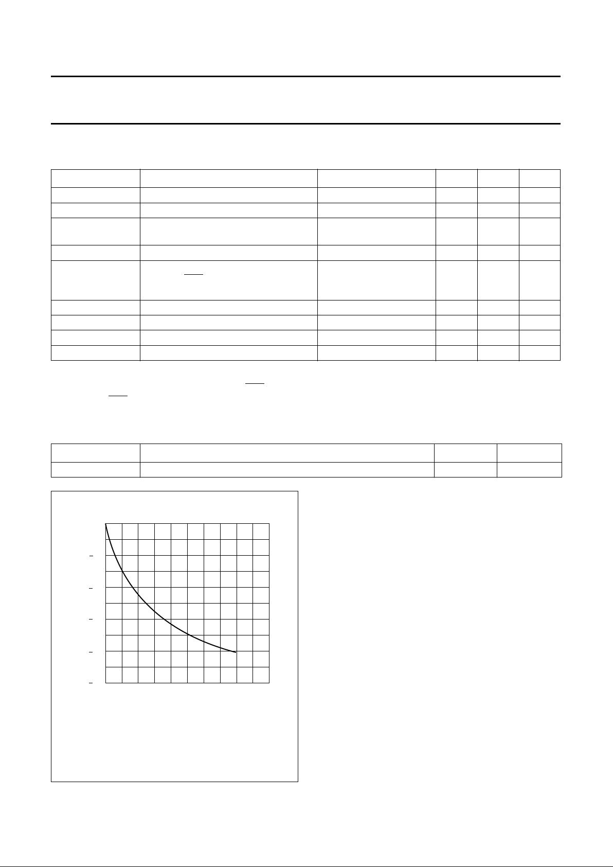
Fig.3 Average effect of air flow on R
th j-a
.
Test conditions: PCB (2.24 ×2.24 ×0.062 inches).
LFPM = Linear Foot Per Minute.
handbook, halfpage
0 1000
0
50
40
MBB851
30
20
10
200 400 600 800
airflow (LFPM)
R
th j-a
(%)
∆
 Loading...