

Philips tda8718 DATASHEETS

INTEGRATED CIRCUITS
DATA SH EET
TDA8718
8-bit high-speed analog-to-digital
converter
Product specification
Supersedes data of April 1993
File under Integrated Circuits, IC02
Philips Semiconductors
June 1994

Philips Semiconductors Product specification
8-bit high-speed analog-to-digital converter TDA8718
FEATURES
• 8-bit resolution
• Sampling rate up to 600 MHz
• ECL (100K family) compatible for digital inputs and
outputs
• Overflow/Underflow output
GENERAL DESCRIPTION
The TDA8718 is an 8-bit analog-to-digital converter (ADC)
designed for professional applications. The device
converts the analog input signal into 8-bit binary coded
digital words at a sampling rate of 600 MHz. It has an
effective bandwidth capability up to 150 MHz full-scale
sine wave. All digital outputs are ECL compatible.
• 50 Ω load drive capability
• Low input capacitance (5 pF typ.).
APPLICATIONS
• High speed analog-to-digital conversion
• Industrial instrumentation
• Data communication
• RF communication.
QUICK REFERENCE DATA
Measured over full voltage and temperature ranges, unless otherwise specified.
SYMBOL PARAMETER CONDITIONS MIN. TYP. MAX. UNIT
V
EEA
V
EED
I
ref
I
EEA
I
EED
I
EEO(L)
I
EEO(H)
analog supply voltage −4.2 −4.5 −4.8 V
digital supply voltage −4.2 −4.5 −4.8 V
resistive ladder current R = 48 Ω 30 45 60 mA
analog supply current 30 42 54 mA
digital supply current 100 120 150 mA
LOW level output supply current RL = 50 Ω 40 70 90 mA
HIGH level output supply current RL = 50 Ω 155 170 185 mA
ILE DC integral linearity error −±0.7 ±1.0 LSB
DLE DC differential linearity error −±0.3 ±0.5 LSB
EB effective bits f
f
clk(max)
P
tot
maximum clock frequency 600 −−MHz
total power dissipation − 990 1250 mW
= 4.43 MHz; I
i
f
= 100 MHz
clk
= 4.43 MHz; I
f
i
f
= 100 MHz
clk
= 45 mA;
ref
= 45 mA;
ref
− 7.5 − bits
− 6.5 − bits
ORDERING INFORMATION
TYPE NUMBER
PINS PIN POSITION MATERIAL CODE
TDA8718K 28 PLCC28 plastic SOT261-2
June 1994 2
PACKAGE
Philips Semiconductors Product specification
8-bit high-speed analog-to-digital converter TDA8718
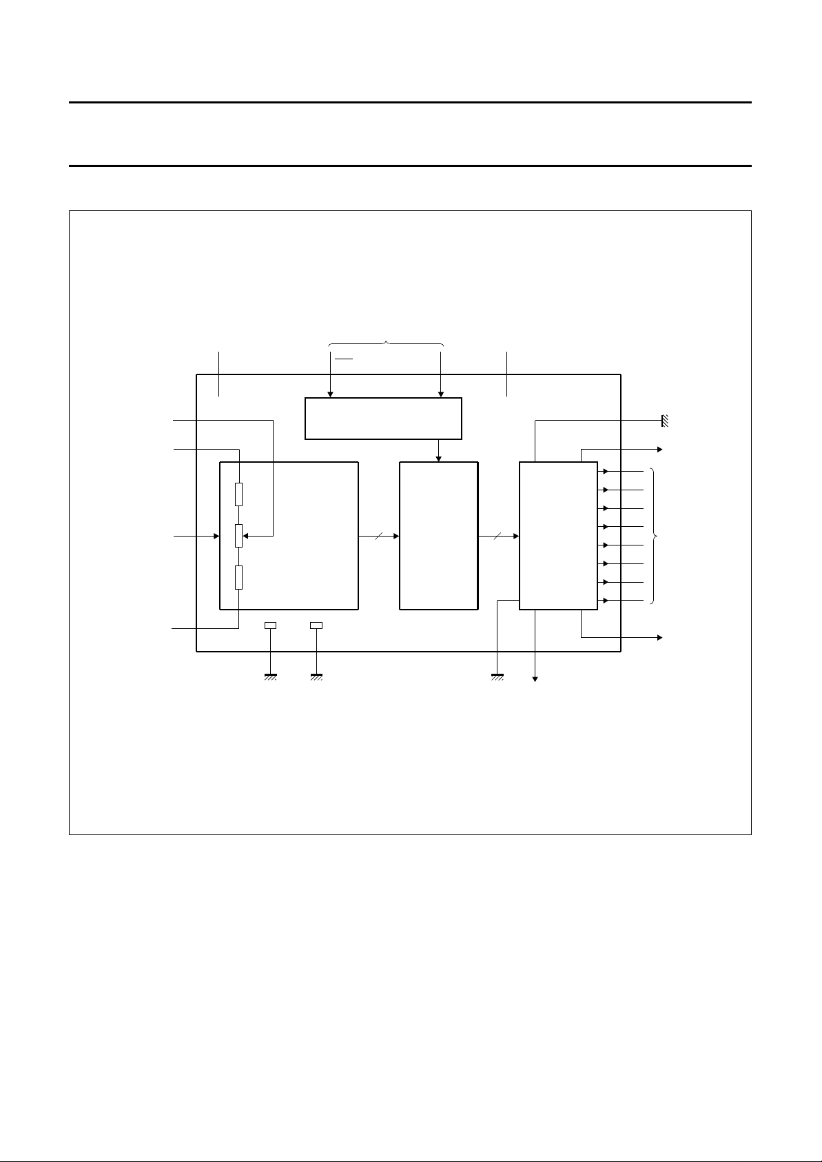
BLOCK DIAGRAM
handbook, full pagewidth
reference
voltage middle
reference
voltage TOP
analog
voltage input
reference
voltage BOTTOM
analog negative
supply voltage
VRM2
V
RT
5
V
3
I
V
1
RB
V
EEA
28
8
Ω
RESISTOR
LADDER
32
Ω
ANALOG SIGNAL
PROCESSING
8
Ω
27
AGND
analog ground digital ground
CLK CLK
CLOCK DRIVER
&
24
DGND
clock inputs
INPUT
AND
OUTPUT
LATCHES
&
DIGITAL
DECODING
digital negative
supply voltage
V
EED
2389
ECL OUTPUTS
12
OGND1
TDA8718
11
V
BB
18
10
13
14
15
16
17 D2
19
20
21
MBB854 - 2
OGND2
6
OF
D7
D6
D5
D4
D3
D1
D0
UF
output
ground
overflow
output
MSB
data outputs
LSB
underflow
output
Fig.1 Block diagram.
June 1994 3

Philips Semiconductors Product specification
8-bit high-speed analog-to-digital converter TDA8718
PINNING
SYMB
OL
V
RB
V
RM
V
I
PIN DESCRIPTION
1 reference voltage BOTTOM
2 reference voltage MIDDLE decoupling
3 analog input voltage
n.c. 4 not connected
V
RT
5 reference voltage TOP
OF 6 overflow digital output
n.c. 7 not connected
CLK 8 clock input
CLK 9 complementary clock input
D7 10 digital output; bit 7 (MSB)
V
BB
11 ECL reference voltage
OGND1 12 output ground 1 (0 V)
D6 13 digital output; bit 6
D5 14 digital output; bit 5
D4 15 digital output; bit 4
D3 16 digital output; bit 3
D2 17 digital output; bit 2
OGND2 18 output ground 2 (0 V)
D1 19 digital output; bit 1
D0 20 digital output; bit 0 (LSB)
UF 21 underflow digital output
n.c. 22 not connected
V
EED
23 digital supply voltage (−4.5 V)
DGND 24 digital ground
n.c. 25 not connected
n.c. 26 not connected
AGND 27 analog ground
V
EEA
28 analog supply voltage (−4.5 V)
handbook, halfpage
V
5
RT
6
OF
7
n.c.
8
CLK
9
CLK
10
D7
V
11
BB
n.c.
4
I
V
3
V
V
V
2
AGND
1
28
27
EEA
RM
RB
TDA8718
12
13
14
15
16
17
D6
OGND1
D5D4D3
D2
Fig.2 Pin configuration.
n.c.
26
18
MBB850 - 2
OGND2
25
n.c.
24
DGND
V
23
EED
n.c.
22
21
UF
D0
20
19
D1
June 1994 4
Philips Semiconductors Product specification
8-bit high-speed analog-to-digital converter TDA8718
LIMITING VALUES
In accordance with the Absolute Maximum Rating System (IEC 134).
SYMBOL PARAMETER CONDITIONS MIN. MAX. UNIT
V
EEA
V
EED
∆V
EE
V
I
∆V
clk(p-p)
I
O
T
stg
T
amb
T
j
analog supply voltage (pin 28) −7.0 +0.3 V
digital supply voltage (pin 23) −7.0 +0.3 V
supply voltage difference between V
and V
EED
EEA
input voltage (pin 3) referenced to AGND V
clock input voltage difference between
CLK and CLK pin 8 to pin 9
referenced to V
note 1
EED
;
−1.00 +1.0 V
EEA
0V
− 2.0 V
(peak-to-peak value)
output current for each digital output − 30 mA
storage temperature −55 +150 °C
operating ambient temperature 0 +70 °C
junction temperature − +150 °C
Note
1. The circuit has two clock inputs CLK and
CLK. Sampling takes place on the falling edge of the clock input signal;
CLK and CLK are two complementary signals.
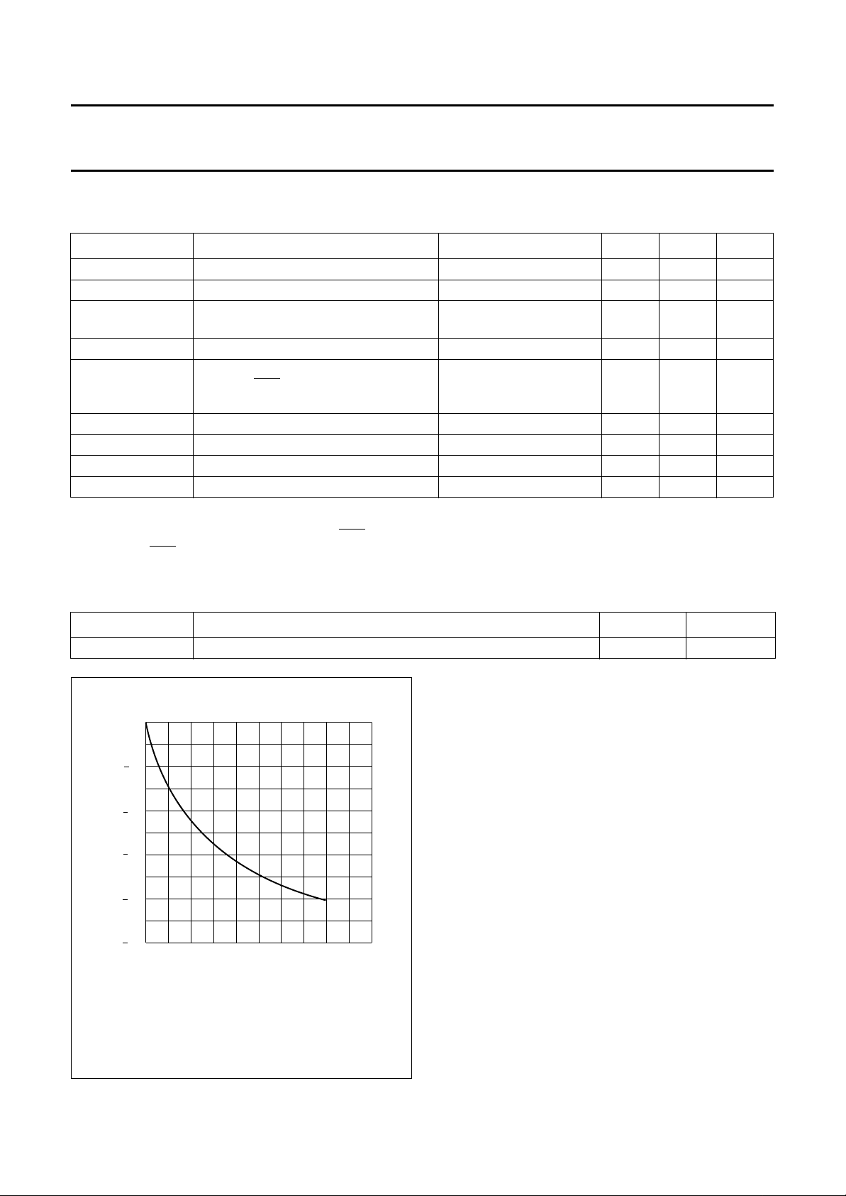
THERMAL CHARACTERISTICS
SYMBOL PARAMETER VALUE UNIT
R
th j-a
handbook, halfpage
R
∆
th j-a
(%)
0
10
20
30
40
thermal resistance from junction to ambient in free air 55 K/W
MBB851
50
Test conditions: PCB (2.24 ×2.24 ×0.062 inches).
LFPM = Linear Foot Per Minute.
Fig.3 Average effect of air flow on R
200 400 600 800
0 1000
airflow (LFPM)
.
th j-a
June 1994 5
 Loading...