

Philips TDA8716T-C1, TDA8716-C1 Datasheet

DATA SH EET
Product specification
Supersedes data of April 1993
File under Integrated Circuits, IC02
1996 Aug 26
INTEGRATED CIRCUITS
TDA8716
8-bit high-speed analog-to-digital
converter

1996 Aug 26 2
Philips Semiconductors Product specification
8-bit high-speed analog-to-digital
converter
TDA8716
FEATURES
• 8-bit resolution
• Sampling rate up to 120 MHz
• ECL (10 K family) compatible digital inputs and outputs
• Overflow/Underflow output
• Low power dissipation
• Low input capacitance (13 pF typ.).
APPLICATIONS
• High speed analog-to-digital convertion
• Video signal digitizing
• Radar pulse analysis
• Transient signal analysis
• High energy physics research
• Medical systems
• Industrial instrumentation.
GENERAL DESCRIPTION
The TDA8716 is an 8-bit high-speed Analog-to-Digital
Converter (ADC) designed for HDTV and professional
applications. The device converts the analog input signal
into 8-bit binary coded digital words at a sampling rate of
120 MHz. All digital outputs are ECL compatible.
QUICK REFERENCE DATA
Measured over full voltage and temperature ranges, unless otherwise specified.
ORDERING INFORMATION
SYMBOL PARAMETER CONDITIONS MIN. TYP. MAX. UNIT
V
EEA
analog supply voltage −5.45 −5.2 −4.95 V
V
EED
digital supply voltage −5.45 −5.2 −4.95 V
I
EEA
analog supply current − 50 55 mA
I
EED
digital supply current − 100 110 mA
I
EEO
output supply current RL = 2.2 kΩ−20 25 mA
V
RB
reference voltage BOTTOM −−3.130 − V
V
RT
reference voltage TOP −−1.870 − V
ILE DC integral linearity error see Fig.8 −±0.5 ±1 LSB
DLE DC differential linearity error see Fig.9 −±0.25 ±0.45 LSB
EB effective bit f
i
= 20 MHz;
f
CLK
= 100 MHz
− 7 − bits
f
CLK
maximum clock frequency 120 −−MHz
P
tot
total power dissipation excluding load − 780 900 mW
TYPE NUMBER
PACKAGE
NAME DESCRIPTION VERSION
TDA8716 DIP24 plastic dual in-line package; 24 leads (600 mil) SOT101-1
TDA8716T SO32L plastic small outline package; 32 leads; body width 7.5 mm SOT287-1
1996 Aug 26 3
Philips Semiconductors Product specification
8-bit high-speed analog-to-digital converter TDA8716
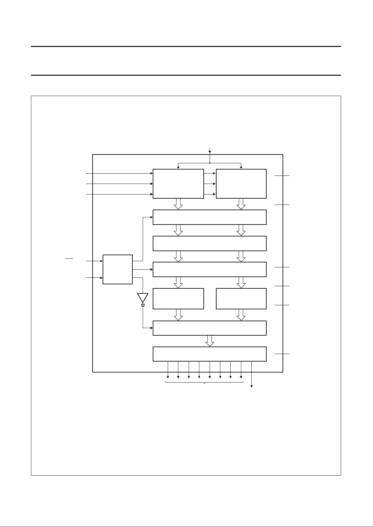
BLOCK DIAGRAM
Fig.1 Block diagram; TDA8716.
handbook, full pagewidth
TDA8716
OUTPUT LATCHES
DIGITAL PROCESSING
LATCHES
CLOCK
BUFFER
MSB ANALOG
PROCESSING
LSB ANALOG
PROCESSING
folding and interpolation
SAMPLE LATCHES
LSB BINARY
ENCODER
MSB BINARY
ENCODER
ECL BUFFERS
63
14 15 16 17 18 20 21 22 23
digital outputs
D0 to D7
IN range
MCD265 - 2
1
2
CLK input
CLKinput
analog input
7
11
5
13
24
3
12
4
19
analog ground
digital ground
analog negative
supply voltage
(– 5.2 V)
output ground
supply voltage
(0 V)
digital negative
supply voltage
(– 5.2 V)
two's complement
output select
10
9
6
8
voltage
reference top
voltage
reference middle
voltage
reference bottom
1996 Aug 26 4
Philips Semiconductors Product specification
8-bit high-speed analog-to-digital converter TDA8716
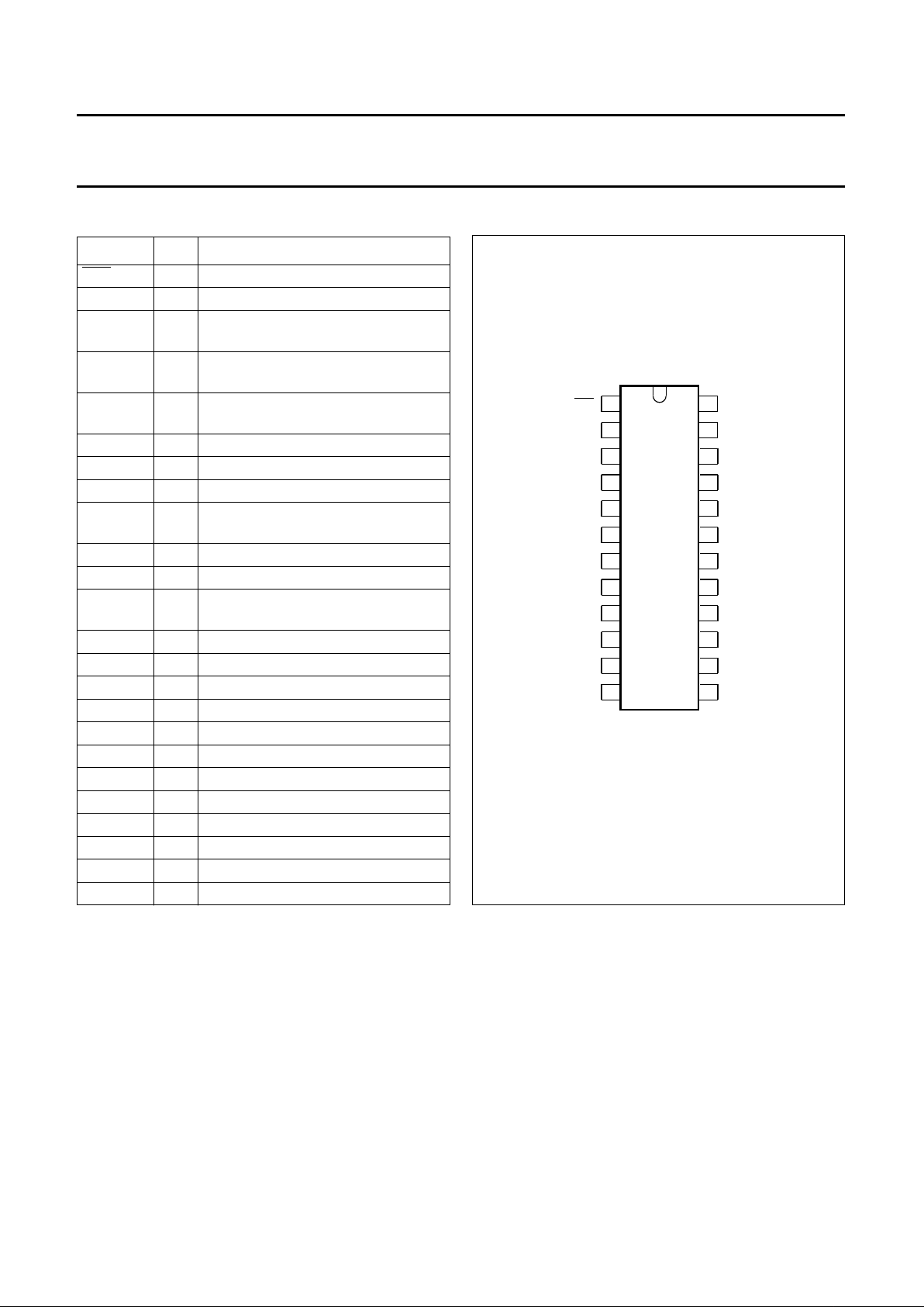
PINNING TDA8716
SYMBOL PIN DESCRIPTION
CLK 1 complementary clock input
CLK 2 clock input
V
EED1
3 digital negative supply voltage
(−5.2 V)
C
PLT2
4 two's complement output select
(active HIGH)
V
EEA
5 analog negative supply voltage
(−5.2 V)
V
RB
6 reference voltage BOTTOM
AGND1 7 analog ground 1
V
I
8 analog input
V
RM
9 reference voltage MIDDLE
decoupling
V
RT
10 reference voltage TOP
AGND2 11 analog ground 2
V
EED2
12 digital negative supply voltage
(−5.2 V)
DGND1 13 digital ground 1
D0 14 digital output (LSB)
D1 15 digital output
D2 16 digital output
D3 17 digital output
D4 18 digital output
OGND 19 output ground supply voltage (0 V)
D5 20 digital output
D6 21 digital output
D7 22 digital output (MSB)
IR 23 IN range
DGND2 24 digital ground 2
Fig.2 Pin configuration; TDA8716.
handbook, halfpage
1
2
3
4
5
6
7
8
9
10
11
12
24
23
22
21
20
19
18
17
16
15
14
13
MCD259
CLK
V
EED1
C
PLT2
AGND1
V
I
EEA
V
AGND2
RM
V
RT
V
RB
V
CLK
DGND2
IR
D7
DGND1
D6
D5
D4
D3
D2
D1
D0
TDA8716
EED2
V
OGND
1996 Aug 26 5
Philips Semiconductors Product specification
8-bit high-speed analog-to-digital converter TDA8716
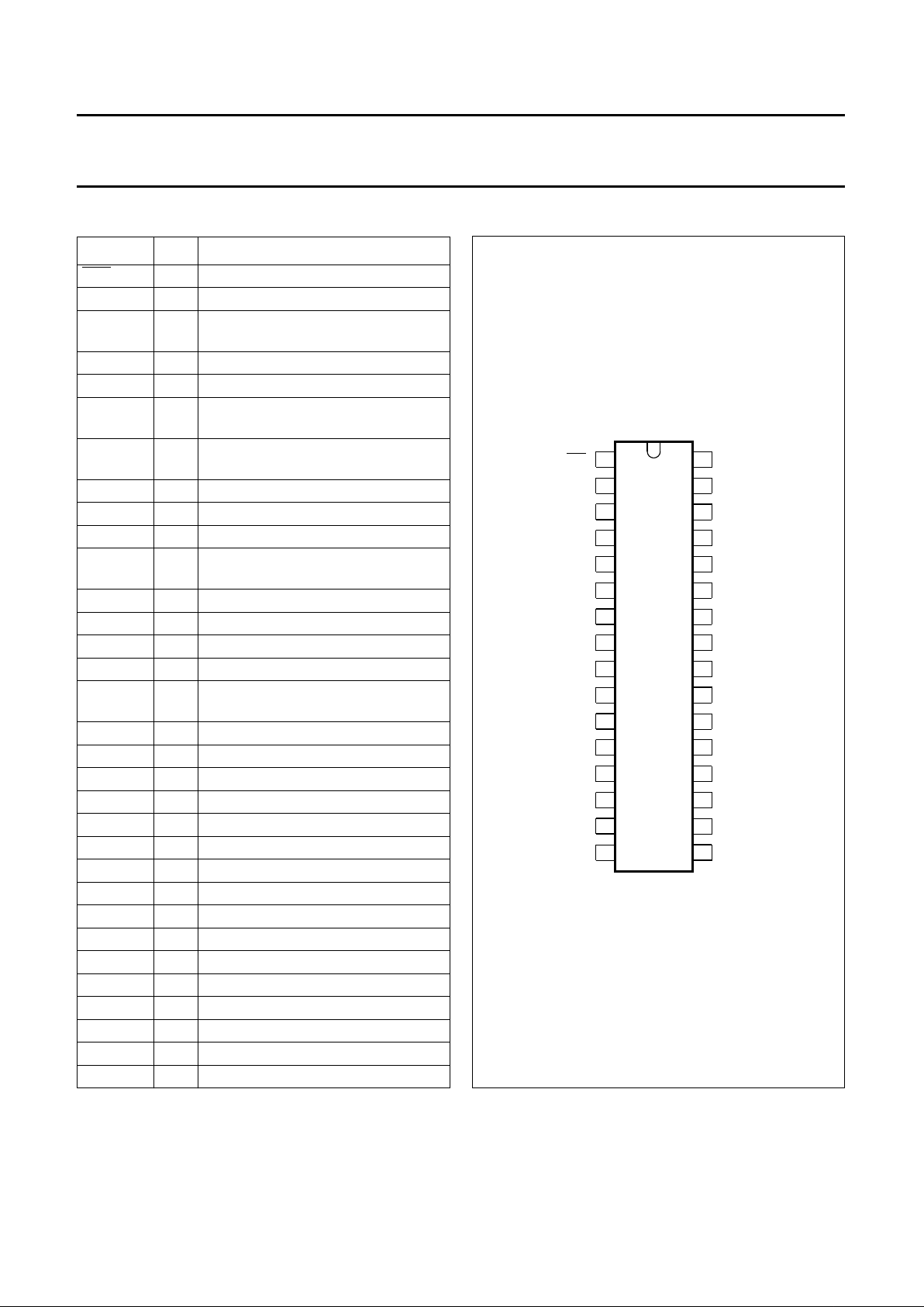
PINNING TDA8716T
SYMBOL PIN DESCRIPTION
CLK 1 complementary clock input
CLK 2 clock input
V
EED1
3 digital negative supply voltage
(−5.2 V)
n.c. 4 not connected
n.c. 5 not connected
C
PLT2
6 two's complement output select
(active HIGH)
V
EEA
7 analog negative supply voltage
(−5.2 V)
V
RB
8 reference voltage BOTTOM
AGND1 9 analog ground 1
V
I
10 analog input
V
RM
11 reference voltage MIDDLE
decoupling
n.c. 12 not connected
n.c. 13 not connected
V
RT
14 reference voltage TOP
AGND2 15 analog ground 2
V
EED2
16 digital negative supply voltage
(−5.2 V)
DGND1 17 digital ground 1
D0 18 digital output (LSB)
D1 19 digital output
n.c. 20 not connected
n.c. 21 not connected
D2 22 digital output
D3 23 digital output
D4 24 digital output
OGND 25 output ground supply voltage (0 V)
D5 26 digital output
D6 27 digital output
n.c. 28 not connected
n.c. 29 not connected
D7 30 digital output (MSB)
IR 31 IN range
DGND2 32 digital ground 2
Fig.3 Pin configuration; TDA8716T.
handbook, halfpage
1
2
3
4
5
6
7
8
9
10
11
12
13
14
15
16
32
31
30
29
28
27
17
18
19
20
21
22
23
24
25
26
TDA8716T
MBC742 - 2
V
EED2
AGND2
V
RT
n.c.
n.c.
RM
V
V
I
AGND1
V
RB
V
EEA
C
PLT2
n.c.
EED1
V
CLK
CLK
DGND1
D0
D1
n.c.
n.c.
D2
D3
D4
OGND
D5
D6
n.c.
n.c.
D7
IR
DGND2
n.c.
1996 Aug 26 6
Philips Semiconductors Product specification
8-bit high-speed analog-to-digital converter TDA8716
LIMITING VALUES
In accordance with the Absolute Maximum Rating System (IEC 134).
Note
1. The circuit has two clock inputs: CLK and
CLK. Sampling takes place on the rising edge of the clock input signal:
CLK and CLK are two's complementary ECL signals.
THERMAL CHARACTERISTICS
HANDLING
Inputs and outputs are protected against electrostatic discharge in normal handling. However, to be totally safe, it is
desirable to take normal precautions appropriate to handling integrated circuits.
SYMBOL PARAMETER CONDITIONS MIN. MAX. UNIT
V
EEA
analog supply voltage −7.0 +0.3 V
V
EED1,VEED2
digital supply voltage −7.0 +0.3 V
V
EEA
− V
EED1
;
V
EEA
− V
EED2
supply voltage differences −1+1V
V
I
input voltage referenced to
AGND
V
EEA
0V
V
CLK; CLK(p-p)
input voltage for differential clock drive
(peak-to-peak value)
note 1 − 2.0 V
I
O
output current (each output stage) − 10 mA
T
stg
storage temperature −55 +150 °C
T
amb
operating ambient temperature 0 +70 °C
T
j
junction temperature − +150 °C
SYMBOL PARAMETER CONDITIONS VALUE UNIT
R
th j-a
from junction to ambient in free air
SOT101 35 K/W
SOT287 (see Fig.4) 65 K/W
1996 Aug 26 7
Philips Semiconductors Product specification
8-bit high-speed analog-to-digital converter TDA8716
CHARACTERISTICS
V
EEA
= −4.95 to −5.45 V; V
EED1
, V
EED2
= −4.95 to −5.45 V; AGND, DGND and OGND shorted together;
T
amb
= 0 to +70 °C; unless otherwise specified. (Typical values taken at V
EEA
= −5.2 V; V
EED1
, V
EED2
= −5.2 V;
T
amb
=25°C).
SYMBOL PARAMETER CONDITIONS MIN. TYP. MAX. UNIT
Supply
V
EEA
analog supply voltage −5.45 −5.2 −4.95 V
V
EED1,VEED2
digital supply voltage −5.45 −5.2 −4.95 V
I
EEA
analog supply current − 50 55 mA
I
EED1,IEED2
digital supply current − 100 110 mA
I
EE
output supply current RL= 2.2 kΩ−20 25 mA
V
diff
supply voltage differential V
EEA
− V
EED1
; V
EEA
− V
EED2
−0.5 0 +0.5 V
Reference voltages for the resistor ladder
V
RB
reference voltage BOTTOM −3.5 −3.13 − V
V
RT
reference voltage TOP −−1.87 −1.5 V
V
ref
reference voltage differential VRT− V
RB
− 1.26 − V
V
OB
voltage offset BOTTOM note 1 − 130 − mV
V
OT
voltage offset TOP note 1 − 130 − mV
V
I(p-p)
input voltage amplitude
(peak-to-peak value)
0.95 1.0 1.5 V
I
ref
reference current − 15 − mA
R
LAD
resistor ladder − 85 −Ω
TC
RL
temperature coefficient of the
resistor ladder
− 0.18 −Ω/K
Inputs
CLK and
CLK input
V
IL
LOW level input voltage −1850 −1770 −1650 mV
V
IH
HIGH level input voltage −960 −880 −810 mV
I
IL
LOW level input current V
CLK
= −1.77 V − 1 −µA
I
IH
HIGH level input current V
CLK
= −0.88 V − 10 −µA
R
I
input resistance − 20 − kΩ
C
I
input capacitance − 2 − pF
V
CLK(p-p)
differential clock input
V
CLK
− V
CLK
(peak-to-peak value)
− 900 − mV
Analog input; note 2
I
IB
input current BOTTOM VRB= −3.13 V − 0 −µA
I
IT
input current TOP VRT= −1.87 V − 170 −µA
R
I
input resistance − 7 − kΩ
C
I
input capacitance − 13 20 pF
 Loading...