Philips tda8542 DATASHEETS

INTEGRATED CIRCUITS
DATA SH EET
TDA8542
2 × 1 W BTL audio amplifier
Preliminary specification
Supersedes data of 1996 Apr 11
File under Integrated Circuits, IC01
1996 May 06

Philips Semiconductors Preliminary specification
2 × 1 W BTL audio amplifier TDA8542
FEATURES
• Flexibility in use
• Few external components
• Low saturation voltage of output stage
• Gain can be fixed with external resistors
• Standby mode controlled by CMOS compatible levels
GENERAL DESCRIPTION
The TDA8542(T) is a two channel audio power amplifier
for an output power of 2 × 1 W with an 8 Ω load at a 5 V
supply. The circuit contains two BTL amplifiers with a
complementary PNP-NPN output stage and standby/mute
logic. The TDA8542T comes in a 16 pin SO package and
the TDA8542 in a 16 pin DIP package.
• Low standby current
• No switch-on/switch-off plops
• High supply voltage ripple rejection
• Protected against electrostatic discharge
• Outputs short-circuit safe to ground, V
CC
and across the
APPLICATIONS
• Portable consumer products
• Personal computers
• Motor-driver (servo).
load
• Thermally protected.
QUICK REFERENCE DATA
SYMBOL PARAMETER CONDITIONS MIN. TYP. MAX. UNIT
V
CC
I
q
I
stb
P
o
THD total harmonic distortion P
supply voltage 2.2 5 18 V
quiescent current VCC=5V − 15 22 mA
standby current −−10 µA
output power THD = 10%; RL=8Ω; VCC=5V 1 −−W
= 0.5 W − 0.15 − %
o
SVRR supply voltage ripple rejection 50 −−dB
ORDERING INFORMATION
TYPE
NUMBER
NAME DESCRIPTION VERSION
PACKAGE
TDA8542T SO16L plastic small outline package; 16 leads; body width 7.5 mm SOT162-1
TDA8541 DIP16 plastic dual in-line package; 16 leads (300 mil); long body SOT38-1
1996 May 06 2

Philips Semiconductors Preliminary specification
2 × 1 W BTL audio amplifier TDA8542
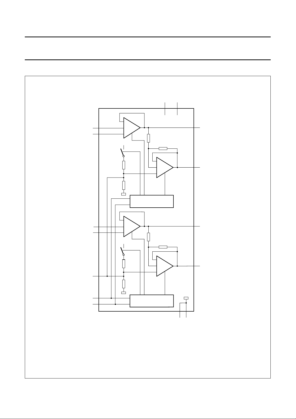
BLOCK DIAGRAM
V
handbook, full pagewidth
CCL
V
CCR
9
16
INL−
INL+
INR−
INR+
SVR
−
14
13
V
CCL
−
+
R
R
15
OUTL−
−
20 kΩ
−
2
OUTL+
+
20 kΩ
STANDBY/MUTE LOGIC
11
12
4
V
−
+
CCR
20 kΩ
20 kΩ
−
TDA8542
R
−
−
+
10
OUTR−
R
7
OUTR+
1996 May 06 3
MODE
BTL/SE
3
5
STANDBY/MUTE LOGIC
LGND
18
RGND
MGB975
Fig.1 Block diagram.

Philips Semiconductors Preliminary specification
2 × 1 W BTL audio amplifier TDA8542
PINNING
SYMBOL PIN DESCRIPTION
LGND 1 ground, left channel
OUTL+ 2 positive loudspeaker terminal,
left channel
MODE 3 operating mode select
(standby, mute, operating)
SVR 4 half supply voltage, decoupling
ripple rejection
BTL/SE 5 BTL loudspeaker or SE
headphone operation
n.c. 6 not connected
OUTR+ 7 positive loudspeaker terminal,
right channel
RGND 8 ground, right channel
V
CCR
9 supply voltage, right channel
OUTR− 10 negative loudspeaker terminal,
right channel
INR− 11 negative input, right channel
INR+ 12 positive input, right channel
INL+ 13 positive input, left channel
INL− 14 negative input, left channel
OUTL− 15 negative loudspeaker terminal,
left channel
V
CCL
16 supply voltage, left channel
FUNCTIONAL DESCRIPTION
The TDA8542(T) is a 2 × 1 W BTL audio power amplifier
capable of delivering 2 × 1 W output power to an 8 Ω load
at THD = 10% using a 5 V power supply. Using the MODE
pin the device can be switched to standby and mute
condition. The device is protected by an internal thermal
shutdown protection mechanism. The gain can be set
within a range from 6 dB to 30 dB by external feedback
resistors.
Power amplifier
The power amplifier is a Bridge Tied Load (BTL) amplifier
with a complementary PNP-NPN output stage. The
voltage loss on the positive supply line is the saturation
voltage of a PNP power transistor, on the negative side the
saturation voltage of a NPN power transistor. The total
voltage loss is <1 V and with a 5 V supply voltage and an
8 Ω loudspeaker an output power of 1 W can be delivered.
Mode select pin
The device is in the standby mode (with a very low current
consumption) if the voltage at the MODE pin is
>(VCC− 0.5 V), or if this pin is floating. At a MODE voltage
level of less than 0.5 V the amplifier is fully operational. In
the range between 1.5 V and VCC− 1.5 V the amplifier is
in mute condition. The mute condition is useful to suppress
plop noise at the output caused by charging of the input
capacitor.
handbook, halfpage
LGND
OUTL+
MODE
SVR
BTL/SE
n.c.
OUTR+
RGND
1
2
3
4
5
6
7
8
TDA8542
MGB974
16
15
14
13
12
11
10
9
V
CCL
OUTL−
INL−
INL+
INR+
INR−
OUTR−
V
CCR
Fig.2 Pin configuration.
1996 May 06 4
Headphone connection
A headphone can be connected to the amplifier using two
coupling capacitors for each channel. The common
GND pin of the headphone is connected to the ground of
the amplifier (see Fig.4). In this case the BTL/SE pin must
be either on a logic HIGH level or not connected at all.
The two coupling capacitors can be omitted if it is allowed
to connect the common GND pin of the headphone jack
1
not to ground, but to a voltage level of
⁄2VCC. See Fig.5 for
the application diagram. In this case the BTL/SE pin must
be either on a logic LOW level or connected to ground. If
the BTL/SE pin is on a LOW level, the power amplifier for
the positive loudspeaker terminal is always in mute
condition.
 Loading...