

Philips TDA8541T-N1-S30, TDA8541T-N1, TDA8541-N1 Datasheet

DATA SH EET
Product specification
Supersedes data of 1997 Feb 19
File under Integrated Circuits, IC01
1998 Apr 01
INTEGRATED CIRCUITS
TDA8541
1 W BTL audio amplifier
1998 Apr 01 2
Philips Semiconductors Product specification
1 W BTL audio amplifier TDA8541
FEATURES
• Flexibility in use
• Few external components
• Low saturation voltage of output stage
• Gain can be fixed with external resistors
• Standby mode controlled by CMOS compatible levels
• Low standby current
• No switch-on/switch-off plops
• High supply voltage ripple rejection
• Protected against electrostatic discharge
• Outputs short-circuit safe to ground, V
CC
and across the
load
• Thermally protected.
GENERAL DESCRIPTION
The TDA8541(T) is a one channel audio power amplifier
for an output power of 1 W with an 8 Ω load at a 5 V
supply. The circuit contains a BTL amplifier with a
complementary PNP-NPN output stage and standby/mute
logic. The TDA8541T comes in an 8 pin SO package and
the TDA8541 in an 8 pin DIP package.
APPLICATIONS
• Portable consumer products
• Personal computers
• Telephony.
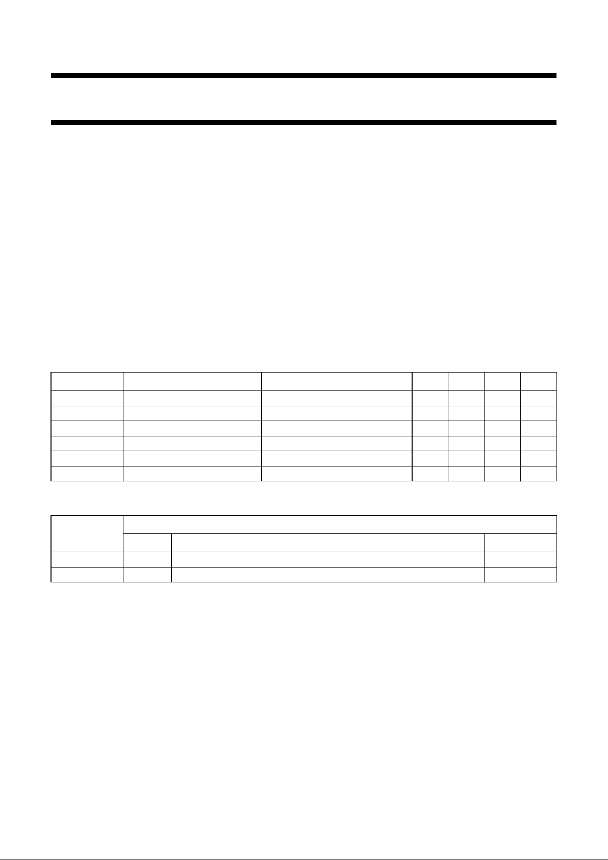
QUICK REFERENCE DATA
ORDERING INFORMATION
SYMBOL PARAMETER CONDITIONS MIN. TYP. MAX. UNIT
V
CC
supply voltage 2.2 5 18 V
I
q
quiescent current VCC=5V − 812mA
I
stb
standby current −−10 µA
P
o
output power THD = 10%; RL=8Ω; VCC=5V 1 1.2 − W
THD total harmonic distortion P
o
= 0.5 W − 0.15 − %
SVRR supply voltage ripple rejection 50 −−dB
TYPE
NUMBER
PACKAGE
NAME DESCRIPTION VERSION
TDA8541T SO8 plastic small outline package; 8 leads; body width 3.9 mm SOT96-1
TDA8541 DIP8 plastic dual in-line package; 8 leads (300 mil) SOT97-1

1998 Apr 01 3
Philips Semiconductors Product specification
1 W BTL audio amplifier TDA8541
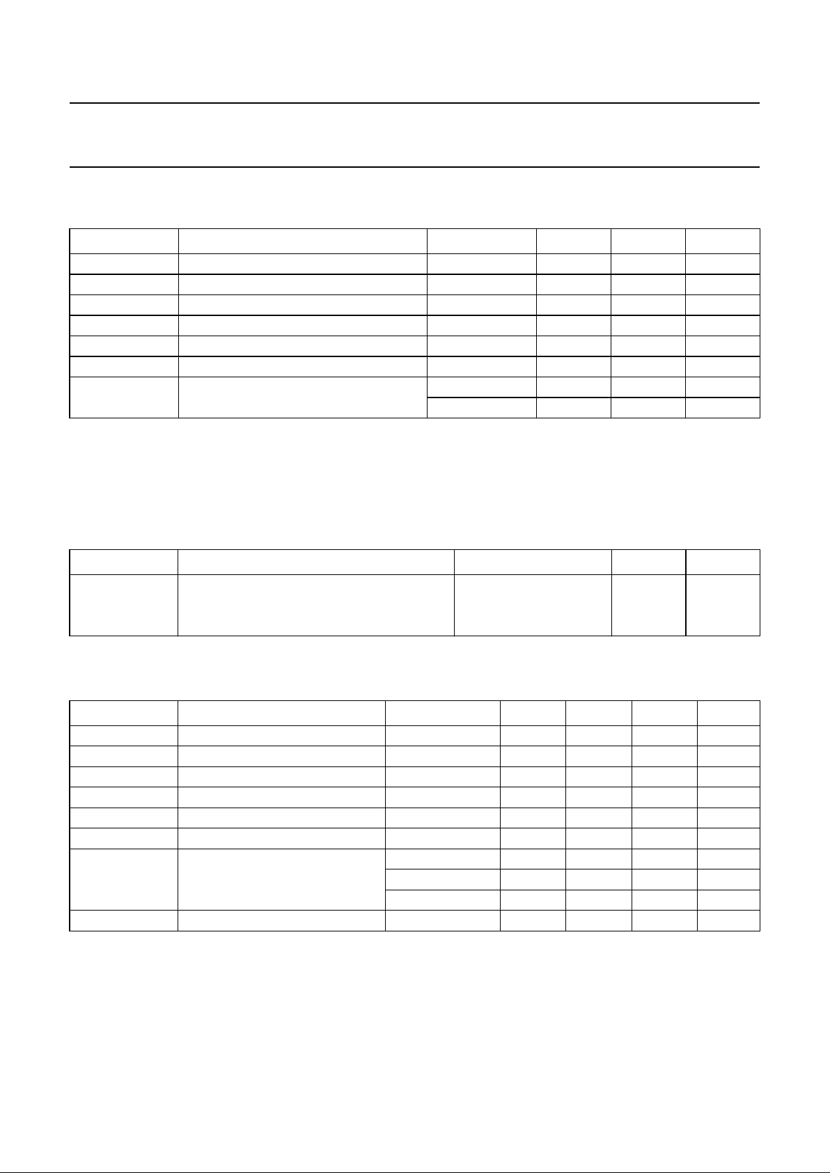
BLOCK DIAGRAM
Fig.1 Block diagram.
handbook, halfpage
MGB972
4
STANDBY/MUTE LOGIC
3
6
2
1
7
8
5
R
R
20 kΩ
20 kΩ
IN−
IN+
V
CC
SVR
MODE
OUT−
OUT+
GND
−
−
+
−
−
+
TDA8541
PINNING
SYMBOL PIN DESCRIPTION
MODE 1 operating mode select
(standby, mute, operating)
SVR 2 half supply voltage, decoupling
ripple rejection
IN+ 3 positive input
IN− 4 negative input
OUT− 5 negative loudspeaker terminal
V
CC
6 supply voltage
GND 7 ground
OUT+ 8 positive loudspeaker terminal
Fig.2 Pin configuration.
handbook, halfpage
1
2
3
4
8
7
6
5
MGB971
TDA8541
OUT+
GNDSVR
V
CC
OUT−
IN−
IN+
MODE
FUNCTIONAL DESCRIPTION
The TDA8541(T) is a BTL audio power amplifier capable
of delivering 1 W output power to an 8 Ω load at
THD = 10% using a 5 V power supply. Using the MODE
pin the device can be switched to standby and mute
condition. The device is protected by an internal thermal
shutdown protection mechanism. The gain can be set
within a range from 6 dB to 30 dB by external feedback
resistors.
Power amplifier
The power amplifier is a Bridge Tied Load (BTL) amplifier
with a complementary PNP-NPN output stage.
The voltage loss on the positive supply line is the
saturation voltage of a PNP power transistor, on the
negative side the saturation voltage of an NPN power
transistor. The total voltage loss is <1 V and with a 5 V
supply voltage and an 8 Ω loudspeaker an output power of
1 W can be delivered.
Mode select pin
The device is in standby mode (with a very low current
consumption) if the voltage at the MODE pin is
>(VCC− 0.5 V), or if this pin is floating. At a MODE voltage
level of less than 0.5 V the amplifier is fully operational.
In the range between 1.5 V and VCC− 1.5 V the amplifier
is in mute condition. The mute condition is useful to
suppress plop noise at the output, caused by charging of
the input capacitor.
1998 Apr 01 4
Philips Semiconductors Product specification
1 W BTL audio amplifier TDA8541
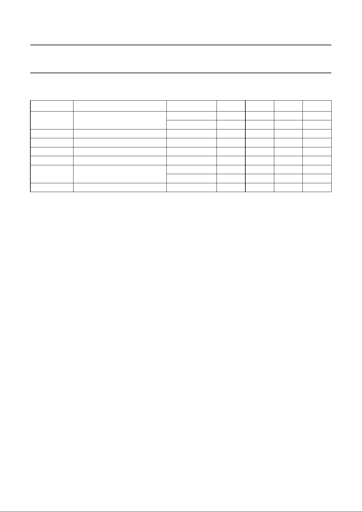
LIMITING VALUES
In accordance with the Absolute Maximum Rating System (IEC 134).
QUALITY SPECIFICATION
In accordance with
“SNW-FQ-611-E”
. The number of the quality specification can be found in the
“Quality Reference
Handbook”
. The handbook can be ordered using the code 9397 750 00192.
THERMAL CHARACTERISTICS
DC CHARACTERISTICS
V
CC
=5V; T
amb
=25°C; RL=8Ω; V
MODE
= 0 V; measured in test circuit Fig.3; unless otherwise specified.
Notes
1. With a load connected at the outputs the quiescent current will increase, the maximum of this increase being equal
to the DC output offset voltage divided by R
L
.
2. The DC output voltage with respect to ground is approximately 0.5 × VCC.
SYMBOL PARAMETER CONDITIONS MIN. MAX. UNIT
V
CC
supply voltage operating −0.3 +18 V
V
I
input voltage −0.3 VCC+ 0.3 V
I
ORM
repetitive peak output current − 1A
T
stg
storage temperature non-operating −55 +150 °C
T
amb
operating ambient temperature −40 +85 °C
V
psc
AC and DC short-circuit safe voltage − 10 V
P
tot
total power dissipation SO8 − 0.8 W
DIP8 − 1.2 W
SYMBOL PARAMETER CONDITIONS VALUE UNIT
R
th j-a
thermal resistance from junction to ambient in free air
TDA8541T (SO8) 160 K/W
TDA8541 (DIP8) 100 K/W
SYMBOL PARAMETER CONDITIONS MIN. TYP. MAX. UNIT
V
CC
supply voltage operating 2.2 5 18 V
I
q
quiescent current RL= ∞; note 1 − 812mA
I
stb
standby current V
MODE=VCC
−−10 µA
V
O
DC output voltage note 2 − 2.2 − V
V
OUT+
− V
OUT−
differential output voltage offset −−50 mV
I
IN+
, I
IN−
input bias current −−500 nA
V
MODE
input voltage mode select operating 0 − 0.5 V
mute 1.5 − V
CC
− 1.5 V
standby V
CC
− 0.5 − V
CC
V
I
MODE
input current mode select 0 < V
MODE<VCC
−−20 µA
1998 Apr 01 5
Philips Semiconductors Product specification
1 W BTL audio amplifier TDA8541
AC CHARACTERISTICS
V
CC
=5V; T
amb
=25°C; RL=8Ω; f = 1 kHz; V
MODE
= 0 V; measured in test circuit Fig.3; unless otherwise specified.
Notes
1. Gain of the amplifier is 2 × R2/R1 in test circuit of Fig.3.
2. The noise output voltage is measured at the output in a frequency range from 20 Hz to 20 kHz (unweighted), with a
source impedance of R
S
=0Ω at the input.
3. Supply voltage ripple rejection is measured at the output, with a source impedance of RS=0Ω at the input.
The ripple voltage is a sine wave with a frequency of 1 kHz and an amplitude of 100 mV (RMS), which is applied to
the positive supply rail.
4. Supply voltage ripple rejection is measured at the output, with a source impedance of RS=0Ω at the input.
The ripple voltage is a sine wave with a frequency between 100 Hz and 20 kHz and an amplitude of 100 mV (RMS),
which is applied to the positive supply rail.
5. Output voltage in mute position is measured with an input voltage of 1 V (RMS) in a bandwidth of 20 kHz, so including
noise.
SYMBOL P ARAMETER CONDITIONS MIN. TYP . MAX. UNIT
P
o
output power THD = 10% 1 1.2 − W
THD = 0.5% 0.6 0.9 − W
THD total harmonic distortion P
o
= 0.5 W − 0.15 0.3 %
G
v
closed loop voltage gain note 1 6 − 30 dB
Z
i
differential input impedance − 100 − kΩ
V
no
noise output voltage note 2 −−100 µV
SVRR supply voltage ripple rejection note 3 50 −−dB
note 4 40 −−dB
V
o
output voltage in mute condition note 5 −−200 µV

1998 Apr 01 6
Philips Semiconductors Product specification
1 W BTL audio amplifier TDA8541
TEST AND APPLICATION INFORMATION
Test conditions
Because the application can be either Bridge-Tied Load
(BTL) or Single-Ended (SE), the curves of each application
are shown separately.
The thermal resistance = 100 K/W for the DIP8 envelope;
the maximum sine wave power dissipation for
T
amb
=25°C is:
.
For T
amb
=60°C the maximum total power dissipation is:
.
BTL application
T
amb
=25°C if not specially mentioned, VCC=5V,
f = 1 kHz, RL=8Ω, Gv= 20 dB, audio band-pass
22 Hz to 22 kHz.
The BTL application diagram is shown in Fig.3.
The quiescent current has been measured without any
load impedance. The total harmonic distortion as a
function of frequency was measured with a low-pass filter
of 80 kHz. The value of capacitor C2 influences the
behaviour of the SVRR at low frequencies, increasing the
value of C2 increases the performance of the SVRR.
The figure of the mode select voltage (Vms) as a function
of the supply voltage shows three areas; operating, mute
and standby. It shows, that the DC-switching levels of the
mute and standby respectively depends on the supply
voltage level.
150 25–
100
----------------------
1.25 W=
150 60–
100
----------------------
0.9 W=
SE application
T
amb
=25°C if not specially mentioned, VCC= 7.5 V,
f = 1 kHz, RL=4Ω, Gv= 20 dB, audio band-pass
22 Hz to 22 kHz.
The SE application diagram is shown in Fig.13.
The capacitor value of C3 in combination with the load
impedance determines the low frequency behaviour.
The total harmonic distortion as a function of frequency
was measured with low-pass filter of 80 kHz. The value of
capacitor C2 influences the behaviour of the SVRR at low
frequencies, increasing the value of C2 increases the
performance of the SVRR.
General remark
The frequency characteristic can be adapted by
connecting a small capacitor across the feedback resistor.
To improve the immunity of HF radiation in radio circuit
applications, a small capacitor can be connected in
parallel with the feedback resistor (56 kΩ); this creates a
low-pass filter.
 Loading...