

Philips TDA8374-N2, TDA8373N-N3, TDA8373C-N3, TDA8373C-N2, TDA8373-N3 Datasheet
...
DATA SH EET
Preliminary specification
File under Integrated Circuits, IC02
1997 Jul 01
INTEGRATED CIRCUITS
TDA837x family
I
2
C-bus controlled economy
PAL/NTSC and NTSC
TV-processors

1997 Jul 01 2
Philips Semiconductors Preliminary specification
I2C-bus controlled economy PAL/NTSC
and NTSC TV-processors
TDA837x family
FEATURES
Available in all ICs:
• Vision IF amplifier with high sensitivity and good figures
for differential phase and gain
• PLL demodulator for the IF signal
• Alignment-free sound demodulator
• Flexible source selection with a CVBS input for the
internal signal and Y/C or CVBS input for the external
signal
• Audio switch
• The output signal of the CVBS (Y/C) switch is externally
available
• Integrated chrominance trap and band-pass filters
(auto-calibrated)
• Luminance delay line integrated
• A symmetrical peaking circuit in the luminance channel
• Black stretching of non-standard CVBS or luminance
signals
• RGB control circuit with black current stabilization and
white point adjustment
• Linear RGB inputs and fast blanking
• Horizontal synchronization with two control loops and
alignment-free horizontal oscillator
• Slow start and slow stop of the horizontal drive pulses
• Vertical count-down circuit
• Vertical driver optimized for DC-coupled vertical output
stages
• I
2
C-bus control of various functions
• Low dissipation
• Small amount of peripheral components compared with
competition ICs.
GENERAL DESCRIPTION
The various versions of the TDA837x series are I
2
C-bus
controlled single-chip TV processors which are intended to
be applied in PAL/NTSC (TDA8374 and TDA8375) and
NTSC (TDA8373 and TDA8377) television receivers.
All ICs are available in an SDIP56 package and some
versions are also available in a QFP64 package. The ICs
are pin compatible so that with one application board
NTSC and PAL/NTSC (or multistandard together with the
SECAM decoder TDA8395) receivers can be built.
Functionally this IC series is split in to 2 categories:
• Versions intended to be used in economy TV receivers
with all basic functions
• Versions with additional functions such as E-W
geometry control, horizontal and vertical zoom function
and YUV interface which are intended for TV receivers
with 110° picture tubes.
The various type numbers are given in Table 1.
The detailed differences between the various ICs are
given in Table 2.
Table 1 TV receiver versions
TV RECEIVERS
SDIP56 PACKAGE QFP64 PACKAGE
ECONOMY MID/HIGH END ECONOMY MID/HIGH END
PAL only TDA8374B − TDA8374BH −
PAL/NTSC (SECAM) TDA8374 and TDA8374A TDA8375 and TDA8375A TDA8374AH TDA8375AH
NTSC TDA8373 TDA8377 and TDA8377A −−
1997 Jul 01 3
Philips Semiconductors Preliminary specification
I2C-bus controlled economy PAL/NTSC
and NTSC TV-processors
TDA837x family
Table 2 Differences between the various ICs
QUICK REFERENCE DATA
CIRCUITS
IC VERSION (TDA)
8373 8374 8374A(H) 8374B(H) 8375 8375A(H) 8377 8377A
Multistandard IF − X −−XX −−
Automatic Volume Levelling
(AVL)
XX − −−− −−
PAL decoder − X X XXX −−
SECAM interface − X X XXX −−
NTSC decoder X X X X X X X X
Colour matrix PAL/NTSC (Japan) − X X XXX −−
Colour matrix NTSC (USA/Japan) X − − −−−XX
YUV interface −− − − XXXX
Horizontal geometry −− − − XXXX
Horizontal and vertical zoom −− − −XX XX
SYMBOL PARAMETER CONDITIONS MIN. TYP. MAX. UNIT
Supplies
V
P
supply voltage − 8.0 − V
I
P
supply current − 110 − mA
Input voltages
V
48,49(rms)
video IF amplifiers sensitivity
(RMS value)
− 70 −µV
V
1(rms)
sound IF amplifiers sensitivity
(RMS value)
− 1.0 − mV
V
2(rms)
external audio input voltage
(RMS value)
− 500 − mV
V
11(p-p)
external CVBS/Y input voltage
(peak-to-peak value)
− 1.0 − V
V
10(p-p)
external chrominance input voltage
(burst amplitude) (peak-to-peak value)
− 0.3 − V
V
23-25(p-p)
RGB input voltage
(peak-to-peak value)
− 0.7 − V
Output signals
V
6(p-p)
IF video output voltage
(peak-to-peak value)
− 2.5 − V
I
54
tuner AGC output current range 0 − 5mA
V
oVSW
output signal level of video switch
(peak-to-peak value)
− 1.0 − V
V
30(p-p)
−(R − Y) output voltage
(peak-to-peak value)
− 525 − mV
1997 Jul 01 4
Philips Semiconductors Preliminary specification
I2C-bus controlled economy PAL/NTSC
and NTSC TV-processors
TDA837x family
ORDERING INFORMATION
V
29(p-p)
−(B − Y) output voltage
(peak-to-peak value)
− 675 − mV
V
28(p-p)
luminance output voltage
(peak-to-peak value)
− 1.4 − V
V
19-21(p-p)
RGB output signal amplitudes
(peak-to-peak value)
− 2.0 − V
I
40
horizontal output current − 10 − mA
I
46,47(p-p)
vertical output current
(peak-to-peak value)
− 1 − mA
I
45(peak)
E-W output current (peak value) TDA8375A,
TDA8377A,
TDA8375 and
TDA8377
− 1.2 − mA
TYPE
NUMBER
PACKAGE
NAME DESCRIPTION VERSION
TDA837xA SDIP56 plastic shrink dual in-line package; 56 leads (600 mil) SOT400-1
TDA837xH QFP64 plastic quad flat package; 64 leads (lead length 1.95 mm);
body 14 × 20 × 2.7 mm; high stand-off height
SOT319-1
SYMBOL PARAMETER CONDITIONS MIN. TYP. MAX. UNIT

1997 Jul 01 5
Philips Semiconductors Preliminary specification
I2C-bus controlled economy PAL/NTSC
and NTSC TV-processors
TDA837x family
BLOCK DIAGRAM
ok, full pagewidth
MGK286
RGB MATRIX
RGB INPUT
AND SWITCH
G - Y MATRIX
AND
SAT CONTROL
NTSC
DECODER
RGB CONTROL
AND
OUTPUT
DELAY
AND
PEAKING
BLACK
STRETCHER
VERTICAL
SYNC
SEPARATOR
TRAP
BLACK
CURRENT
STABILIZER
VERTICAL
GEOMETRY
HORIZONTAL/
VERTICAL
DIVIDER
SYNC
SEPARATOR
AND 1st LOOP
VCO
AND
CONTROL
2nd LOOP AND
HORIZONTAL
OUTPUT
CONTROL DACs
1 × 8 BITS
14 × 6 BITS
1 × 4 BITS
2331
322930
43 14
44 12 37
REF
8753
9 42 4154
3436336161110381713
39
3
3.6
MHz
3
21
18
52
51
22
20
46
50
40
47
19
white
point
BRI
TDA8373
SAT
REF
B−Y
R−Y
HUE
CONTR
24 25 26
FILTER
TUNING
BAND-PASS
SW
SW
56
1
55245
15
49
5
MUTE
VOL SW
CVBS Y/C
SWITCH
PRE-AMPLIFIER
AND MUTE
MUTE
IDENT
ADJ
tuner
take-over
point
+8 V
AFC
VIDEO
AMPLIFIER
AND MUTE
VIDEO
IDENTIFICATION
AGC FOR IF
AND TUNER
I
2
C-BUS
TRANSCEIVER
48
4
3
VIF AMPLIFIER
AND PLL
DEMODULATOR
VCO
ADJUSTMENT
CVBS
SWITCH
AVL AND
SWITCH AND
VOLUME CONTROL
AFC
PLL
DEMODULATOR
SOUND
TRAP
SOUND
BAND-PASS
LIMITER
Fig.1 Block diagram of bus-controlled economy NTSC TV-processor TDA8373.
The TDA8373 is only supplied in an SDIP package.
1997 Jul 01 6
Philips Semiconductors Preliminary specification
I2C-bus controlled economy PAL/NTSC
and NTSC TV-processors
TDA837x family
k, full pagewidth
MGK287
RGB MATRIX
RGB INPUT
AND SWITCH
G - Y MATRIX
AND
SAT CONTROL
PAL/NTSC
DECODER
RGB CONTROL
AND
OUTPUT
DELAY
AND
PEAKING
BLACK
STRETCHER
VERTICAL
SYNC
SEPARATOR
TRAP
BLACK
CURRENT
STABILIZER
VERTICAL
GEOMETRY
HORIZONTAL/
VERTICAL
DIVIDER
SYNC
SEPARATOR
AND 1st LOOP
VCO
AND
CONTROL
2nd LOOP AND
HORIZONTAL
OUTPUT
CONTROL DACs
1 × 8 BITS
14 × 6 BITS
1 × 4 BITS
23
31
322930
43 14
44 12 37
REF
87
53
9 42 41
54
34
(51)
35
36336161110381713
39
3
3.6
MHz
3
21
18
52
51
22
20
46
50
40
47
19
white
point
BRI
TDA8374
SAT
REF
B−Y
R−Y
HUE
CONTR
24 25 26
4.4
MHz
FILTER
TUNING
BAND-PASS
SW
SW
56
1
55245
15
49
5
MUTE
VOL SW
CVBS Y/C
SWITCH
PRE-AMPLIFIER
AND MUTE
MUTE
IDENT
ADJ
tuner
take-over
point
POL
+8 V
AFC
POL
VIDEO
AMPLIFIER
AND MUTE
VIDEO
IDENTIFICATION
AGC FOR IF
AND TUNER
I
2
C-BUS
TRANSCEIVER
48
4
3
VIF AMPLIFIER
AND PLL
DEMODULATOR
VCO
ADJUSTMENT
CVBS
SWITCH
AVL AND
SWITCH AND
VOLUME CONTROL
AFC
PLL
DEMODULATOR
SOUND
TRAP
TDA4665
SOUND
BAND-PASS
LIMITER
Fig.2 Block diagram of bus-controlled economy PAL/NTSC TV processor TDA8374.
For most pins the QFP64 pinning is not indicated.

1997 Jul 01 7
Philips Semiconductors Preliminary specification
I2C-bus controlled economy PAL/NTSC
and NTSC TV-processors
TDA837x family
ok, full pagewidth
MGK288
RGB MATRIX
RGB INPUT
AND SWITCH
G - Y MATRIX
AND
SAT CONTROL
PAL/NTSC
DECODER
RGB CONTROL
AND
OUTPUT
DELAY PLUS
PEAKING PLUS
CORING
BLACK
STRETCHER
VERTICAL
SYNC
SEPARATOR
TRAP
BLACK
CURRENT
STABILIZER
VERTICAL
GEOMETRY
HORIZONTAL/
VERTICAL
DIVIDER
SYNC
SEPARATOR
AND 1st LOOP
VCO
AND
CONTROL
2nd LOOP AND
HORIZONTAL
OUTPUT
CONTROL DACs
1 × 8 BITS
18 × 6 BITS
1 × 4 BITS
(35)
23
(47)
31
(40)
28
(39)
27
(48)
32
(45)
29
(46)
30
43
(59)
14
(25,26)
44
(60,61)
12
(22,23)
37
(53)
REF
8
(18)
7
(17)
53
(6)
9
(19)
42
(58)
41
(57)
40
(56)
54
(7)
(50)
34
(51)
35
(52)
36
(49)
33
(16)
6
(28)
16
(21)
11
(20)
10
(54)
38
(29)
17
(24)
13
(55)
39
3
3.6
MHz
3
(33) 21
(30) 18
(5) 52
(4) 51
(34) 22
(32) 20
(63) 46
(3) 50
E-W
GEOMETRY
(62) 45
(64) 47
(31) 19
white
point
BRI
TDA8375
SAT
REF
B−Y
R−Y
HUE
CONTR
(36)
24
(37)
25
(38)
26
4.4
MHz
FILTER
TUNING
BAND-PASS
SW
SW
56 (9)
1 (10)
55 (8)
2 (11)
15 (27)
49 (2)
5 (15)
MUTE
VOL SW
CVBS Y/C
SWITCH
PRE-AMPLIFIER
AND MUTE
MUTE
IDENT
ADJ
tuner
take-over
point
POL
+8 V
AFC
POL
VIDEO
AMPLIFIER
AND MUTE
VIDEO
IDENTIFICATION
AGC FOR IF
AND TUNER
I
2
C-BUS
TRANSCEIVER
48 (1)
4 (14)
3 (13)
VIF AMPLIFIER
AND PLL
DEMODULATOR
VCO
ADJUSTMENT
CVBS
SWITCH
SWITCH AND
VOLUME CONTROL
AFC
PLL
DEMODULATOR
SOUND
TRAP
TDA4665
SOUND
BAND-PASS
LIMITER
Fig.3 Block diagram of bus-controlled economy PAL/NTSC TV processor TDA8375.
1997 Jul 01 8
Philips Semiconductors Preliminary specification
I2C-bus controlled economy PAL/NTSC
and NTSC TV-processors
TDA837x family
ull pagewidth
MGK289
RGB MATRIX
RGB INPUT
AND SWITCH
G - Y MATRIX
AND
SAT CONTROL
NTSC
DECODER
RGB CONTROL
AND
OUTPUT
DELAY PLUS
PEAKING PLUS
CORING
BLACK
STRETCHER
VERTICAL
SYNC
SEPARATOR
TRAP
BLACK
CURRENT
STABILIZER
VERTICAL
GEOMETRY
HORIZONTAL/
VERTICAL
DIVIDER
SYNC
SEPARATOR
AND 1st LOOP
VCO
AND
CONTROL
2nd LOOP AND
HORIZONTAL
OUTPUT
CONTROL DACs
1 × 8 BITS
18 × 6 BITS
1 × 4 BITS
23
31
28 27
322930
43 14
44 12 37
REF
87
53
9 42 41 40
54
3436336161110381713
39
3
3.6
MHz
3
21
18
52
51
22
20
46
50
E-W
GEOMETRY
45
47
19
white
point
BRI
TDA8377
SAT
REF
B−Y
R−Y
HUE
CONTR
24 25 26
FILTER
TUNING
BAND-PASS
SW
SW
56
1
55215
49
5
MUTE
VOL SW
CVBS Y/C
SWITCH
PRE-AMPLIFIER
AND MUTE
MUTE
IDENT
ADJ
tuner
take-over
point
+8 V
AFC
VIDEO
AMPLIFIER
AND MUTE
VIDEO
IDENTIFICATION
AGC FOR IF
AND TUNER
I
2
C-BUS
TRANSCEIVER
48
4
3
VIF AMPLIFIER
AND PLL
DEMODULATOR
VCO
ADJUSTMENT
CVBS
SWITCH
SWITCH AND
VOLUME CONTROL
AFC
PLL
DEMODULATOR
SOUND
TRAP
SOUND
BAND-PASS
LIMITER
Fig.4 Block diagram of bus-controlled economy NTSC TV processor TDA8377.
The TDA8377 is only supplied in an SDIP package.

1997 Jul 01 9
Philips Semiconductors Preliminary specification
I2C-bus controlled economy PAL/NTSC
and NTSC TV-processors
TDA837x family
PINNING
SYMBOL
PIN
DESCRIPTION
SDIP56 QFP64
SIF 1 10 sound IF input
AUDI 2 11 external audio input
VCO1 3 13 IF VCO 1 tuned circuit
VCO2 4 14 IF VCO 2 tuned circuit
PLL 5 15 PLL loop filter
IFVO 6 16 IF video output
SCL 7 17 serial clock input (I
2
C-bus)
SDA 8 18 serial data input/output (I
2
C-bus)
DEC
BG
9 19 band gap decoupling
CHROMA 10 20 chrominance input
CVBS/Y 11 21 CVBS/Y input
V
P1
12 22 and 23 main supply voltage (+8 V)
CVBS
int
13 24 internal CVBS input
GND1 14 25 and 26 ground
AUDO 15 27 audio output
DEC
FT
16 28 decoupling filter tuning
CVBS
ext
17 29 external CVBS input
BLKIN 18 30 black current input
BO 19 31 blue output
GO 20 32 green output
RO 21 33 red output
BCLIN 22 34 beam current input
RI 23 35 red input
GI 24 36 green input
BI 25 37 blue input
RGBIN 26 38 RGB insertion input
YIN 27
(2)
39 luminance input
YOUT 28 40 luminance output
BYO 29 45 (B −Y) output
RYO 30 46 (R − Y) output
RYI 31 47 (R − Y) input
BYI 32 48 (B − Y) input
SEC
ref
33
(1)
49 SECAM reference output
XTAL1 34 50 3.58 MHz crystal connection
XTAL2 35
(1)
51 4.43 MHz crystal connection
LFBP 36 52 loop filter burst phase detector
V
P2
37 53 horizontal oscillator supply voltage (+8 V)
CVBSO 38 54 CVBS output

1997 Jul 01 10
Philips Semiconductors Preliminary specification
I2C-bus controlled economy PAL/NTSC
and NTSC TV-processors
TDA837x family
Notes
1. In the TDA8373 and TDA8377 pin 35 (4.43 MHz crystal) is internally connected and pin 33 is just a subcarrier output
which can be used as a reference signal for comb filter ICs.
2. In the TDA8373 and TDA8374 the following pins are different (SDIP56): Pin 27: not connected; Pin 45: AVL
capacitor.
BLPH 39 55 black peak hold capacitor
HOUT 40 56 horizontal drive output
FBI/SCO 41 57 flyback input and sandcastle output
PH2 42 58 phase 2 filter/protection
PH1 43 59 phase 1 filter
GND2 44 60 and 61 ground 2
EWD 45
(2)
62 east-west drive output
VDOB 46 63 vertical drive output B
VDOA 47 64 vertical drive output A
IFIN1 48 1 IF input 1
IFIN2 49 2 IF input 2
EHT/PRO 50 3 EHT/overvoltage protection input
VSAW 51 4 vertical sawtooth capacitor
I
ref
52 5 reference current input
DEC
AGC
53 6 AGC decoupling capacitor
AGCOUT 54 7 tuner AGC output
AUDEEM 55 8 audio deemphasis
DEC 56 9 decoupling sound demodulator
i.c. − 12 internally connected
i.c. − 41 internally connected
i.c. − 42 internally connected
i.c. − 43 internally connected
i.c. − 44 internally connected
SYMBOL
PIN
DESCRIPTION
SDIP56 QFP64
1997 Jul 01 11
Philips Semiconductors Preliminary specification
I2C-bus controlled economy PAL/NTSC
and NTSC TV-processors
TDA837x family
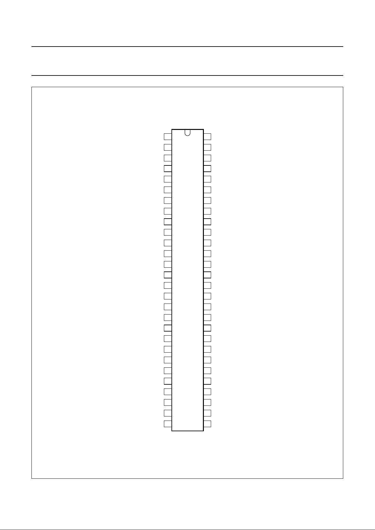
Fig.5 Pin configuration (SDIP56).
handbook, halfpage
TDA837x
MGK284
1
2
3
4
5
6
7
8
9
10
11
12
13
14
15
16
17
18
19
20
21
22
23
24
25
26
52
51
50
55
56
54
53
49
48
47
46
45
44
43
42
41
40
39
38
37
36
35
34
33
32
31
30
29
27
28
SIF
AUDI
VCO1
VCO2
PLL
IFVO
SCL
SDA
DEC
BG
CHROMA
CVBS/Y
V
P1
CVBS
int
GND1
AUDO
DEC
FT
CVBS
ext
BLKIN
BO
GO
RO
BCLIN
RI
GI
BI
RGBIN
YIN
YOUT
DEC
AUDEEM
AGCOUT
DEC
AGC
I
ref
VSAW
EHT/PRO
IFIN2
IFIN1
VDOA
VDOB
EWD
GND2
PH1
PH2
FBI/SCO
HOUT
BLPH
CVBSO
V
P2
LFBP
XTAL2
XTAL1
SEC
ref
BYI
RYI
RYO
BYO

1997 Jul 01 12
Philips Semiconductors Preliminary specification
I2C-bus controlled economy PAL/NTSC
and NTSC TV-processors
TDA837x family
Fig.6 Pin configuration (QFP64).
handbook, full pagewidth
TDA837xH
MGK285
1
2
3
4
5
6
7
8
9
10
11
12
13
14
15
16
48
47
46
45
44
43
42
41
40
39
38
37
36
35
34
BYI
RYI
RYO
BYO
i.c.
i.c.
i.c.
i.c.
YOUT
YIN
RGBIN
BI
GI
RI
BCLIN
RO
IFIN1
IFIN2
EHT/PRO
VSAW
I
ref
DEC
AGC
AGCOUT
AUDEEM
DEC
SIF
AUDI
i.c.
VCO1
VCO2
PLL
IFVO 33
17
18
19
20
21
22
23
24
25
26
27
28
29
30
31
32
64
63
62
61
60
59
58
57
56
55
54
53
52
51
50
VDOA
VDOB
EWD
GND2
GND2
PH1
PH2
FBI/SCO
HOUT
BLPH
CVBSO
VP2LFBP
XTAL2
XTAL1
SEC
ref
SCL
SDA
DEC
BG
CHROMA
CVBS/Y
VP1V
P1
CVBS
int
GND1
GND1
AUDO
DEC
FT
CVBS
ext
BLKIN
BO
GO 49

1997 Jul 01 13
Philips Semiconductors Preliminary specification
I2C-bus controlled economy PAL/NTSC
and NTSC TV-processors
TDA837x family
FUNCTIONAL DESCRIPTION
Vision IF amplifier
The IF amplifier contains 3 AC-coupled control stages with
a total gain control range which is higher than 66 dB.
The sensitivity of the circuit is comparable with that of
modern IF-ICs.
The video signal is demodulated by a PLL carrier
regenerator. This circuit contains a frequency detector and
a phase detector. During acquisition the frequency
detector will tune the VCO to the correct frequency.
The initial adjustment of the oscillator is realized via the
I
2
C-bus.
The switching, between SECAM L and L’, can also be
realized via the I2C-bus. After lock-in the phase detector
controls the VCO so that a stable phase relationship
between the VCO and the input signal is achieved.
The VCO operates at twice the IF frequency.
The reference signal for the demodulator is obtained by
using a frequency divider circuit.
The AFC output is obtained by using the VCO control
voltage of the PLL and can be read via the I2C-bus.
For fast search tuning systems the window of the AFC can
be increased by a factor of 3. The setting is realized with
the AFW bit.
Depending on the device type the AGC detector operates
on top-sync level (single standard versions) or on top-sync
and top-white level (multistandard versions).
The demodulation polarity is switched via the I2C-bus.
The AGC detector time constant capacitor is connected
externally. This is mainly because of the flexibility of the
application. The time constant of the AGC system during
positive modulation is rather long, this is to avoid visible
variations of the signal amplitude. To improve the speed of
the AGC system, a circuit has been included which detects
whether the AGC detector is activated every frame period.
When, during 3 frame periods, no action is detected the
speed of the system is increased. For signals without
peak-white information the system switches automatically
to a gated black level AGC. Because a black level clamp
pulse is required for this method of operation the circuit will
only switch to black level AGC in the internal mode.
The circuits contain a second fast video identification
circuit which is independent of the synchronization
identification circuit. Consequently, search tuning is also
possible when the display section of the receiver is used
as a monitor. However, this identification circuit cannot be
made as sensitive as the slower sync identification circuit
(SL) and it is recommended to use both identification
outputs to obtain a reliable search system.
The identification output is applied to the tuning system via
the I
2
C-bus.
The input of the identification circuit is connected to pin 13,
the internal CVBS input (see Fig.1). This has the
advantage that the identification circuit can also be made
operative when a scrambled signal is received
[descrambler connected between the IF video output
(pin 6) and pin 13]. A second advantage is that the
identification circuit can be used when the IF amplifier is
not used (e.g. with built-in satellite tuners).
The video identification circuit can also be used to identify
the selected CBVS or Y/C signal. The switching between
the two modes can be realized with bit VIM.
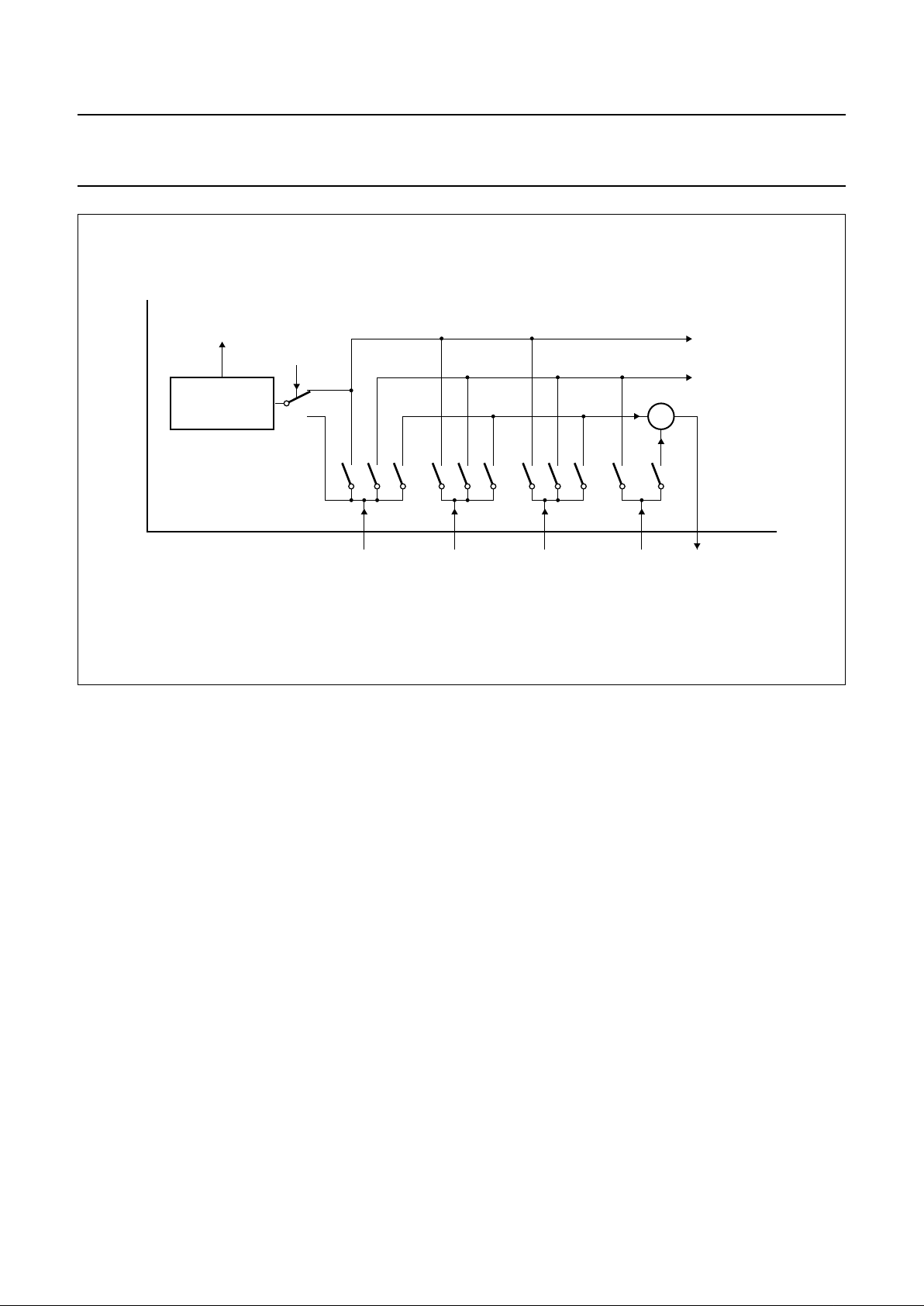
Video switches
The circuit has two CVBS inputs (CVBS
int
and CVBS
ext
)
and a Y/C input. When the Y/C input is not required pin 11
can be used as the third CVBS input. The switch
configuration is illustrated in Fig.7. The selection of the
various sources is made via the I2C-bus.
The output signal of the CVBS switch is externally
available and can be used to drive the teletext decoder, the
SECAM add-on decoder and a comb filter.
In applications with comb filters a Y/C input is only possible
when additional switches are added. In applications
without comb filters the Y/C input signal can be switched
to the CVBS output.
1997 Jul 01 14
Philips Semiconductors Preliminary specification
I2C-bus controlled economy PAL/NTSC
and NTSC TV-processors
TDA837x family
Fig.7 Configuration CVBS switch and interfacing of video identification.
handbook, full pagewidth
MGK301
VIDEO
IDENTIFICATION
S0
VIM
IDENT
TDA837x
CVBS
int
13
S0 S5
S1
CVBS
ext
17
S1 S6 S2
CVBS/Y
11
S3 S7 S4
CHROMA CVBSO
10 38
to luminance/
sync processing
to chrominance
processing
S8
+
Sound circuit
The sound band-pass and trap filters have to be
connected externally. The filtered intercarrier signal is fed
to a limiter circuit and is demodulated by a PLL
demodulator. This PLL circuit automatically tunes to the
incoming carrier signal, hence no adjustment is required.
The volume is controlled via the I2C-bus. The de-emphasis
capacitor has to be connected externally.
The non-controlled audio signal can be obtained from this
pin (pin 55) (via a buffer stage).
The FM demodulator can be muted via the I
2
C-bus. This
function can be used to switch-off the sound during a
channel change so that high output peaks are prevented
(also on the de-emphasis output).
The TDA8373 and TDA8374 contain an Automatic Volume
Levelling (AVL) circuit which automatically stabilizes the
audio output signal to a certain level which can be set by
the user via the volume control. This function prevents big
audio output fluctuations due to variations of the
modulation depth of the transmitter. The AVL function can
be activated via the I2C-bus.
Synchronization circuit
The sync separator is preceded by a controlled amplifier
which adjusts the sync pulse amplitude to a fixed level.
These pulses are fed to the slicing stage which operates at
50% of the amplitude.
The separated sync pulses are fed to the first phase
detector and to the coincidence detector. The coincidence
detector is used to detect whether the line oscillator is
synchronized and can also be used for transmitter
identification. The circuit can be made less sensitive by
using the STM bit. This mode can be used during search
tuning to ensure that the tuning system will not stop at very
weak input signals. The first PLL has a very high static
steepness so that the phase of the picture is independent
of the line frequency.
The line oscillator operates at twice the line frequency.
The oscillator capacitor is internal. Because of the spread
of internal components an automatic calibration circuit has
been added to the IC. The circuit compares the oscillator
frequency with that of the crystal oscillator in the colour
decoder.

1997 Jul 01 15
Philips Semiconductors Preliminary specification
I2C-bus controlled economy PAL/NTSC
and NTSC TV-processors
TDA837x family
This results in a free-running frequency which deviates
less than 2% from the typical value. When the IC is
switched on the horizontal output signal is suppressed and
the oscillator is calibrated as soon as all subaddress bytes
have been sent. When the frequency of the oscillator is
correct the horizontal drive signal is switched on. To obtain
a smooth switching on and switching off behaviour of the
horizontal output stage the horizontal output frequency is
doubled during switch-on and switch-off (slow start/stop).
During that time the duty cycle of the output pulse has such
a value that maximum safety is obtained for the output
stage.
To protect the horizontal output transistor, the horizontal
drive is immediately switched off (via the slow stop
procedure) when a power-on reset is detected. The drive
signal is switched on again when the normal switch-on
procedure is followed, i.e. all subaddress bytes must be
sent and, after calibration, the horizontal drive signal will
be released again via the slow start procedure.
When the coincidence detector indicates an out-of-lock
situation the calibration procedure is repeated.
The circuit has a second control loop to generate the drive
pulses for the horizontal driver stage. The horizontal
output is gated with the flyback pulse so that the horizontal
output transistor cannot be switched on during the flyback
time.
Adjustments can be made to the horizontal shift, vertical
shift, vertical slope, vertical amplitude and the S-correction
via the I2C-bus. In the TDA8375A, TDA8377A, TDA8375
and TDA8377 the E-W drive can also be adjusted via the
I2C-bus. The TDA8375 and TDA8377 have a flexible zoom
adjustment possibility for the vertical and horizontal
deflection. When the horizontal scan is reduced to display
4 : 3 pictures on a 16 : 9 picture tube an accurate video
blanking can be switched on to obtain well defined edges
on the screen. The geometry processor has a differential
output for the vertical drive signal and a single-ended
output for the E-W drive (TDA8375A, TDA8377A,
TDA8375 and TDA8377). Overvoltage conditions (X-ray
protection) can be detected via the EHT tracking pin.
When an overvoltage condition is detected the horizontal
output drive signal will be switched off via the slow stop
procedure. However, it is also possible that the drive is not
switched off and that just a protection indication is given in
the I2C-bus output byte. The choice is made via the input
bit PRD. The ICs have a second protection input on the
phase-2 filter capacitor pin. When this input is activated the
drive signal is switched off immediately (without slow stop)
and switched on again via the slow start procedure.
For this reason this protection input can be used as ‘flash
protection’.
The drive pulses for the vertical sawtooth generator are
obtained from a vertical countdown circuit. This countdown
circuit has various windows depending on the incoming
signal (50 or 60 Hz and standard or non-standard).
The countdown circuit can be forced in various modes via
the I2C-bus. To obtain short switching times of the
countdown circuit during a channel change the divider can
be forced in the search window using the NCIN bit.
The vertical deflection can be set in the de-interlace mode
via the I2C-bus.
To avoid damage of the picture tube when the vertical
deflection fails, the guard output current of the TDA8350
and TDA8351 can be supplied to the beam current limiting
input. When a failure is detected the RGB outputs are
blanked and a bit is set (NDF) in the status byte of the
I2C-bus. When no vertical deflection output stage is
connected this guard circuit will also blank the output
signals. This can be overruled using the EVG bit.
Chrominance and luminance processing
The circuit contains a chrominance band-pass and trap
circuit. The filters are realized by using gyrator circuits.
They are automatically calibrated by comparing the tuning
frequency with the crystal frequency of the decoder.
The luminance delay line and the delay for the peaking
circuit are also realized by using gyrator circuits.
The centre frequency of the chrominance band-pass filter
is 10% higher than the subcarrier frequency. This
compensates for the high frequency attenuation of the IF
saw filter. During SECAM reception the centre frequency
of the chrominance trap is reduced to obtain a better
suppression of the SECAM carrier frequencies. All ICs
have a black stretcher circuit which corrects the black level
for incoming video signals which have a deviation between
the black level and the blanking level (back porch).
The TDA8375A, TDA8377A, TDA8375 and TDA8377
have a defeatable coring function in the peaking circuit.
Some of the ICs have a YUV interface so that picture
improvement ICs such as the TDA9170 (contrast
improvement), TDA9177 (sharpness improvement) and
TDA4556 and TDA4566 (CTI) can be applied. When the
TDA4556 or TDA4566 is applied it is possible to increase
the gain of the luminance channel by using the GAI bit in
subaddress 03 so that the resulting RGB output signals
will not be affected.

1997 Jul 01 16
Philips Semiconductors Preliminary specification
I2C-bus controlled economy PAL/NTSC
and NTSC TV-processors
TDA837x family
Colour decoder
Depending on the IC type the colour decoder can decode
NTSC signals (TDA8373 and TDA8377) or PAL/NTSC
signals (TDA8374 and TDA8375). The circuit contains an
alignment-free crystal oscillator, a killer circuit and two
colour difference demodulators. The 90° phase shift for the
reference signal is made internally.
The TDA8373 and TDA8377 contain an Automatic Colour
Limiting (ACL) circuit which prevents over saturation
occurring when signals with a high chroma-to-burst ratio
are received. This ACL function is also available in the
TDA8374 and TDA8375, however, it is only active during
the reception of NTSC signals.
The TDA8373 and TDA8377 have a switchable colour
difference matrix (via the I
2
C-bus) so that the colour
reproduction can be adapted to the market requirements.
In the TDA8374 and TDA8375 the colour difference matrix
switches automatically between PAL and NTSC, however,
it is also possible to fix the matrix in the PAL standard.
The TDA8374 and TDA8375 can operate in conjunction
with the SECAM decoder TDA8395 so that an automatic
multistandard decoder can be realized. The subcarrier
reference output for the SECAM decoder can also be used
as a reference signal for a comb filter. Consequently, the
reference signal is continuously available when PAL or
NTSC signals are detected and only present during the
vertical retrace period when a SECAM signal is detected.
Which standard the TDA8374 and TDA8375 can decode
depends on the external crystals. The crystal to be
connected to pin 34 must have a frequency of 3.5 MHz
(NTSC-M, PAL-M or PAL-N). Pin 35 can handle crystals
with a frequency of 4.4 and 3.5 MHz. Because the crystal
frequency is used to tune the line oscillator, the value of
the crystal frequency must be communicated to the IC via
the I2C-bus. It is also possible to use the IC in the so called
‘3-norma’ mode for South America. In that event one
crystal must be connected to pin 35 and the other two to
pin 34. Switching between the 2 latter crystals must be
performed externally. Consequently, the search loop of the
decoder must be controlled by the microcontroller.
To prevent calibration problems of the horizontal oscillator
the external switching between the two crystals should be
performed when the oscillator is forced to pin 35.
For a reliable calibration of the horizontal oscillator it is
very important that the crystal indication bits (XA and XB)
are not corrupted. For this reason the crystal bits can be
read in the output bytes so that the software can check the
I
2
C-bus transmission.
RGB output circuit and black current stabilization
The colour difference signals are matrixed with the
luminance signal to obtain the RGB signals. Linear
amplifiers have been chosen for the RGB inputs so that the
circuit is suited for signals that are input from the SCART
connector. The insertion blanking can be switched on or off
using the IE1 bit. To ascertain whether the insertion pin
has a (continuous) HIGH level or not can be read via the
IN1 bit. The contrast and brightness control operate on
internal and external signals.
The output signal has an amplitude of approximately 2 V
(black-to-white) at nominal input signals and nominal
settings of the controls. To increase the flexibility of the IC
it is possible to add OSD and/or teletext signals directly at
the RGB outputs. This insertion mode is controlled via the
insertion input. The action to switch the RGB outputs to
black has some delay which must be compensated for
externally.
The black current stabilization is realized by using a
feedback from the video output amplifiers to the RGB
control circuit. The black current of the 3 guns of the
picture tube is internally measured and stabilized.
The black level control is active during 4 lines at the end of
the vertical blanking. The vertical blanking is adapted to
the incoming CVBS signal (50 or 60 Hz). When the flyback
time of the vertical output stage is longer than the 60 Hz
blanking time, or when additional lines need to be blanked
(e.g. for close captioning lines) the blanking can be
increased to the same value as that of the 50 Hz blanking.
This can be set using the LBM bit. The leakage current is
measured during the first line and, during the following
3 lines, the 3 guns are adjusted to the required level.
The maximum acceptable leakage current is ±100 µA.
The nominal value of the black current is 10 µA. The ratio
of the currents for the various guns automatically tracks
with the white point adjustment so that the background
colour is the same as the adjusted white point.

1997 Jul 01 17
Philips Semiconductors Preliminary specification
I2C-bus controlled economy PAL/NTSC
and NTSC TV-processors
TDA837x family
The input impedance of the black current measuring pin is
14 kΩ. To prevent the voltage on this pin exceeding the
supply voltage during scan an internal protection diode
has been included.
When the TV receiver is switched on the black current
stabilization circuit is not active, the RGB outputs are
blanked and the beam current limiting input pin is
short-circuited. Only during the measuring lines will the
outputs supply a voltage of 4.2 V to the video output stage
to ascertain whether the picture tube is warming up. As
soon as the current supplied to the measuring input
exceeds a value of 190 µA the stabilization circuit will be
activated. After a waiting time of approximately 0.8 s the
blanking and beam current limiting input pins are released.
The remaining switch-on behaviour of the picture is
determined by the external time constant of the beam
current limiting network.
I
2
C-bus specification
Table 3 Slave address (8A)
A6 A5 A4 A3 A2 A1 A0 R/W
1000101I/O
The slave address is identical for all types. The
subaddresses of the various types are slightly different.
The list of subaddresses for each type is given in
Tables 4, 6, 8 and 10.
S
TART-UP PROCEDURE
Read the status bytes until POR = 0 and send all
subaddress bytes. The horizontal output signal is switched
on when the oscillator is calibrated. Each time before the
data in the IC is refreshed, the status bytes must be read.
If POR = 1, then the procedure given above must be
carried out to restart the IC. When this procedure is not
followed the horizontal frequency in the TDA8374 and
TDA8375 may be incorrect after power-up or a power dip.
1997 Jul 01 18
Philips Semiconductors Preliminary specification
I2C-bus controlled economy PAL/NTSC
and NTSC TV-processors
TDA837x family
TDA8373
Valid subaddresses: 00 to 16 (subaddresses 04 to 07 are not used), subaddress FE is reserved for test purposes.
Auto-increment mode available for subaddresses.
Table 4 Inputs
Table 5 Output status bytes (note 1)
Note
1. X = don’t care.
FUNCTION
SUB
ADDRESS
DATA BYTE
D7 D6 D5 D4 D3 D2 D1 D0
Control 0 00 INA INB INC 0 FOA FOB 0 0
Control 1 01 0 0 DL STB POC 0 1 1
Hue 02 AVL AKB A5 A4 A3 A2 A1 A0
Horizontal Shift (HS) 03 VIM GAI A5 A4 A3 A2 A1 A0
Vertical Slope (VS) 08 NCIN STM A5 A4 A3 A2 A1 A0
Vertical Amplitude (VA) 09 VID LBM A5 A4 A3 A2 A1 A0
S-Correction (SC) 0A 0 EVG A5 A4 A3 A2 A1 A0
Vertical shift (VSH) 0B SBL PRD A5 A4 A3 A2 A1 A0
White point R 0C 0 0 A5 A4 A3 A2 A1 A0
White point G 0D 0 0 A5 A4 A3 A2 A1 A0
White point B 0E MAT 0 A5 A4 A3 A2 A1 A0
Peaking 0F 0000A3A2A1A0
Brightness 10 RBL 0 A5 A4 A3 A2 A1 A0
Saturation 11 IE1 0 A5 A4 A3 A2 A1 A0
Contrast 12 AFW IFS A5 A4 A3 A2 A1 A0
AGC takeover 13 0 VSW A5 A4 A3 A2 A1 A0
Volume control 14 SM FAV A5 A4 A3 A2 A1 A0
Adjustment IF-PLL 15 L’FA A6 A5 A4 A3 A2 A1 A0
Spare 16 00000000
OUTPUT ADDRESS D7 D6 D5 D4 D3 D2 D1 D0
00 POR X X SL XPR CD2 CD1 CD0
01 NDF IN1 X IFI AFA AFB SXA SXB
02 X X X IVW X ID2 ID1 ID0

1997 Jul 01 19
Philips Semiconductors Preliminary specification
I2C-bus controlled economy PAL/NTSC
and NTSC TV-processors
TDA837x family
TDA8374, TDA8374AH and TDA8374BH
Valid subaddresses: 00 to 16 (subaddresses 04 to 07 are not used), subaddress FE is reserved for test purposes.
Auto-increment mode available for subaddresses.
Table 6 Inputs (notes 1 and 2)
Notes
1. The AVL and MOD bit are not available in the TDA8374A.
2. In the TDA8374B the AVL and MOD bit is also missing and the CM0 to CM2 and CD0 to CD2 bits have less
possibilities because this IC can only decode PAL or PAL/SECAM signals (when the TDA8395 is applied).
Table 7 Output status bytes (note 1)
Note
1. X = don’t care.
FUNCTION
SUB
ADDRESS
DATA BYTE
D7 D6 D5 D4 D3 D2 D1 D0
Control 0 00 INA INB INC 0 FOA FOB XA XB
Control 1 01 FORF FORS DL STB POC CM2 CM1 CM0
Hue 02 AVL AKB A5 A4 A3 A2 A1 A0
Horizontal Shift (HS) 03 VIM GAI A5 A4 A3 A2 A1 A0
Vertical Slope (VS) 08 NCIN STM A5 A4 A3 A2 A1 A0
Vertical Amplitude (VA) 09 VID LBM A5 A4 A3 A2 A1 A0
S-Correction (SC) 0A 0 EVG A5 A4 A3 A2 A1 A0
Vertical shift (VSH) 0B SBL PRD A5 A4 A3 A2 A1 A0
White point R 0C 0 0 A5 A4 A3 A2 A1 A0
White point G 0D 0 0 A5 A4 A3 A2 A1 A0
White point B 0E MAT 0 A5 A4 A3 A2 A1 A0
Peaking 0F 0000A3A2A1A0
Brightness 10 RBL 0 A5 A4 A3 A2 A1 A0
Saturation 11 IE1 0 A5 A4 A3 A2 A1 A0
Contrast 12 AFW IFS A5 A4 A3 A2 A1 A0
AGC takeover 13 MOD VSW A5 A4 A3 A2 A1 A0
Volume control 14 SM FAV A5 A4 A3 A2 A1 A0
Adjustment IF-PLL 15 L’FA A6 A5 A4 A3 A2 A1 A0
Spare 16 00000000
OUTPUT ADDRESS D7 D6 D5 D4 D3 D2 D1 D0
00 POR FSI X SL XPR CD2 CD1 CD0
01 NDF IN1 X IFI AFA AFB SXA SXB
02 X X X IVW X ID2 ID1 ID0

1997 Jul 01 20
Philips Semiconductors Preliminary specification
I2C-bus controlled economy PAL/NTSC
and NTSC TV-processors
TDA837x family
TDA8375 and TDA8375AH
Valid subaddresses: 00 to 16, subaddress FE is reserved for test purposes. Auto-increment mode available for
subaddresses.
Table 8 Inputs
Note
1. The vertical zoom byte and the HBL bit are active only in the TDA8375.
Table 9 Output status bytes (note 1)
Note
1. X = don’t care.
FUNCTION
SUB
ADDRESS
DATA BYTE
D7 D6 D5 D4 D3 D2 D1 D0
Control 0 00 INA INB INC 0 FOA FOB XA XB
Control 1 01 FORF FORS DL STB POC CM2 CM1 CM0
Hue 02 HBL AKB A5 A4 A3 A2 A1 A0
Horizontal Shift (HS) 03 VIM GAI A5 A4 A3 A2 A1 A0
E-W width (EW) 04 0 0 A5 A4 A3 A2 A1 A0
E-W Parabola/Width (PW) 05 0 0 A5 A4 A3 A2 A1 A0
E-W Corner Parabola (CP) 06 0 0 A5 A4 A3 A2 A1 A0
E-W trapezium (TC) 07 0 0 A5 A4 A3 A2 A1 A0
Vertical Slope (VS) 08 NCIN STM A5 A4 A3 A2 A1 A0
Vertical Amplitude (VA) 09 VID LBM A5 A4 A3 A2 A1 A0
S-Correction (SC) 0A HCO EVG A5 A4 A3 A2 A1 A0
Vertical shift (VSH) 0B SBL PRD A5 A4 A3 A2 A1 A0
White point R 0C 0 0 A5 A4 A3 A2 A1 A0
White point G 0D 0 0 A5 A4 A3 A2 A1 A0
White point B 0E MAT 0 A5 A4 A3 A2 A1 A0
Peaking 0F 0000A3A2A1A0
Brightness 10 RBL COR A5 A4 A3 A2 A1 A0
Saturation 11 IE1 0 A5 A4 A3 A2 A1 A0
Contrast 12 AFW IFS A5 A4 A3 A2 A1 A0
AGC takeover 13 MOD VSW A5 A4 A3 A2 A1 A0
Volume control 14 SM FAV A5 A4 A3 A2 A1 A0
Adjustment IF-PLL 15 L’FA A6 A5 A4 A3 A2 A1 A0
Vertical zoom (VX)
(1)
16 0 0 A5 A4 A3 A2 A1 A0
OUTPUT ADDRESS D7 D6 D5 D4 D3 D2 D1 D0
00 POR FSI X SL XPR CD2 CD1 CD0
01 NDF IN1 X IFI AFA AFB SXA SXB
02 X X X IVW X ID2 ID1 ID0

1997 Jul 01 21
Philips Semiconductors Preliminary specification
I2C-bus controlled economy PAL/NTSC
and NTSC TV-processors
TDA837x family
TDA8377 and TDA8377A
Valid subaddresses: 00 to 16, subaddress FE is reserved for test purposes. Auto-increment mode available for
subaddresses.
Table 10 Inputs
Note
1. The vertical zoom byte and the HBL bit are active only in the TDA8377.
Table 11 Output status bytes (note 1)
Note
1. X = don’t care.
FUNCTION
SUB
ADDRESS
DATA BYTE
D7 D6 D5 D4 D3 D2 D1 D0
Control 0 00 INA INB INC 0 FOA FOB 0 1
Control 1 01 0 0 DL STB POC 0 1 1
Hue 02 HBL AKB A5 A4 A3 A2 A1 A0
Horizontal Shift (HS) 03 VIM GAI A5 A4 A3 A2 A1 A0
E-W width (EW) 04 0 0 A5 A4 A3 A2 A1 A0
E-W Parabola/Width (PW) 05 0 0 A5 A4 A3 A2 A1 A0
E-W Corner Parabola (CP) 06 0 0 A5 A4 A3 A2 A1 A0
E-W trapezium (TC) 07 0 0 A5 A4 A3 A2 A1 A0
Vertical Slope (VS) 08 NCIN STM A5 A4 A3 A2 A1 A0
Vertical Amplitude (VA) 09 VID 0 A5 A4 A3 A2 A1 A0
S-Correction (SC) 0A HCO EVG A5 A4 A3 A2 A1 A0
Vertical shift (VSH) 0B SBL PRD A5 A4 A3 A2 A1 A0
White point R 0C 0 0 A5 A4 A3 A2 A1 A0
White point G 0D 0 0 A5 A4 A3 A2 A1 A0
White point B 0E MAT 0 A5 A4 A3 A2 A1 A0
Peaking 0F 0000A3A2A1A0
Brightness 10 RBL COR A5 A4 A3 A2 A1 A0
Saturation 11 IE1 0 A5 A4 A3 A2 A1 A0
Contrast 12 AFW IFS A5 A4 A3 A2 A1 A0
AGC takeover 13 0 VSW A5 A4 A3 A2 A1 A0
Volume control 14 SM FAV A5 A4 A3 A2 A1 A0
Adjustment IF-PLL 15 L’FA A6 A5 A4 A3 A2 A1 A0
Vertical zoom (VX)
(1)
16 0 0 A5 A4 A3 A2 A1 A0
OUTPUT ADDRESS D7 D6 D5 D4 D3 D2 D1 D0
00 POR X X SL XPR CD2 CD1 CD0
01 NDF IN1 X IFI AFA AFB SXA SXB
02 X X X IVW X ID2 ID1 ID0

1997 Jul 01 22
Philips Semiconductors Preliminary specification
I2C-bus controlled economy PAL/NTSC
and NTSC TV-processors
TDA837x family
INPUT CONTROL BITS
Table 12 Source select
Table 13 Phase 1 (ϕ-1) time constant
Table 14 Crystal indication
Table 15 Forced field frequency TDA8374 and TDA8375
Note
1. When switched to this mode while locked to a 50 Hz signal, the divider will only switch to forced 60 Hz when an
out-of-sync is detected in the horizontal PLL.
INA INB INC
SELECTED SIGNALS
(DECODER AND AUDIO)
SWITCH OUTPUT
0 0 0 internal CVBS plus audio internal CVBS
0 0 1 external CVBS plus audio external CVBS
0 1 0 Y/C plus external audio Y/C (Y plus C)
0 1 1 CVBS3 plus external audio CVBS3
1 0 0 Y/C plus internal audio internal CVBS
1 1 0 Y/C plus external audio external CVBS
FOA FOB MODE
0 0 normal
0 1 slow and gated
1 0 slow/fast and gated
1 1 fast
XA XB CRYSTAL
0 0 two 3.6 MHz crystals
0 1 one 3.6 MHz crystal (pin 34)
1 0 one 4.4 MHz crystal (pin 35)
1 1 3.6 MHz and 4.4 MHz crystals (pins 34 and 35)
FORF FORS FIELD FREQUENCY
0 0 auto (60 Hz when line not synchronized)
0 1 60 Hz; note 1
1 0 keep last detected field frequency
1 1 auto (50 Hz when line not synchronized)
 Loading...