Philips tda8310a DATASHEETS

INTEGRATED CIRCUITS
DATA SH EET
TDA8310A
PAL/NTSC colour processor
for PIP applications
Product specification
Supersedes data of 1995 Nov 29
File under Integrated Circuits, IC02
1996 Jan 25

Philips Semiconductors Product specification
PAL/NTSC colour processor
for PIP applications
FEATURES
• Video switch with 2 CVBS inputs. One input can be
switched between CVBS and Y/C and the circuit can
automatically detect whether the incoming signal is
CVBS or Y/C
• Integrated chrominance trap and bandpass filters
(automatically calibrated)
• Integrated luminance delay line
• Automatic PAL/NTSC decoder which can decode all
standards available in the world
• Easy interfacing with the TDA8395 (SECAM decoder)
for multistandard applications
• Horizontal PLL with an alignment-free horizontal
oscillator
• Vertical count-down circuit
• RGB/YUV and fast blanking switch with 3-state output
and active clamping
• Low dissipation (560 mW)
• Small amount of peripheral components compared with
competition ICs.
TDA8310A
GENERAL DESCRIPTION
The TDA8310A is an alignment-free PAL/NTSC colour
processor for Picture-in-Picture (PIP) applications.
The main difference between the TDA8310 and the
TDA8310A is that the vision IF amplifier has been omitted
in the TDA8310A. Therefore, the circuit contains an input
signal selector, a PAL/NTSC colour decoder, horizontal
and vertical synchronization and an RGB/YUV switch.
The input signal selector has 2 CVBS inputs. One of the
inputs can be switched between CVBS and Y/C and the
circuit can automatically detect whether the incoming
signal is CVBS or Y/C. The output signals for the PIP
processor are;
Luminance signal
Colour difference signals (U and V)
Horizontal and vertical synchronization pulses.
The RGB/YUV switch can select between two RGB or
YUV sources, e.g. between the PIP processor and the
SCART input signal.
The supply voltage for the IC is 8 V. It is available in a
52-pin SDIP package.
ORDERING INFORMATION
TYPE NUMBER
NAME DESCRIPTION VERSION
TDA8310A SDIP52 plastic shrink dual in-line package; 52 leads (600 mil) SOT247-1
PACKAGE
1996 Jan 25 2

Philips Semiconductors Product specification
PAL/NTSC colour processor
TDA8310A
for PIP applications
QUICK REFERENCE DATA
SYMBOL PARAMETER MIN. TYP. MAX. UNIT
V
P
I
P
Input voltages
V
17,20(p-p)
V
16(p-p)
V
i(p-p)
Output signals
V
o(p-p)
V
50(p-p)
V
51(p-p)
V
39
V
36
G
v
Control voltage
V
control
supply voltage (pins 19 and 41) 7.2 8.0 8.8 V
supply current − 70 1.4 mA
CVBS/Y input voltage (peak-to-peak value) − 1.0 − V
chrominance input voltage (peak-to-peak value) − 0.3 − V
RGB/YUV input signal voltage amplitude
−−1.3 V
(peak-to-peak value)
luminance output voltage (peak-to-peak value) − 1.4 − V
(B−Y) output voltage (peak-to-peak value) 1.06 1.33 1.6 V
(R−Y) output voltage (peak-to-peak value) 0.84 1.05 1.26 V
horizontal sync pulse output voltage − 4.0 − V
vertical sync pulse output voltage − 4.0 − V
voltage gain of the RGB switches −0.5 0 +0.5 dB
control voltage for HUE 0 − 5.0 V
1996 Jan 25 3

Philips Semiconductors Product specification
PAL/NTSC colour processor
for PIP applications
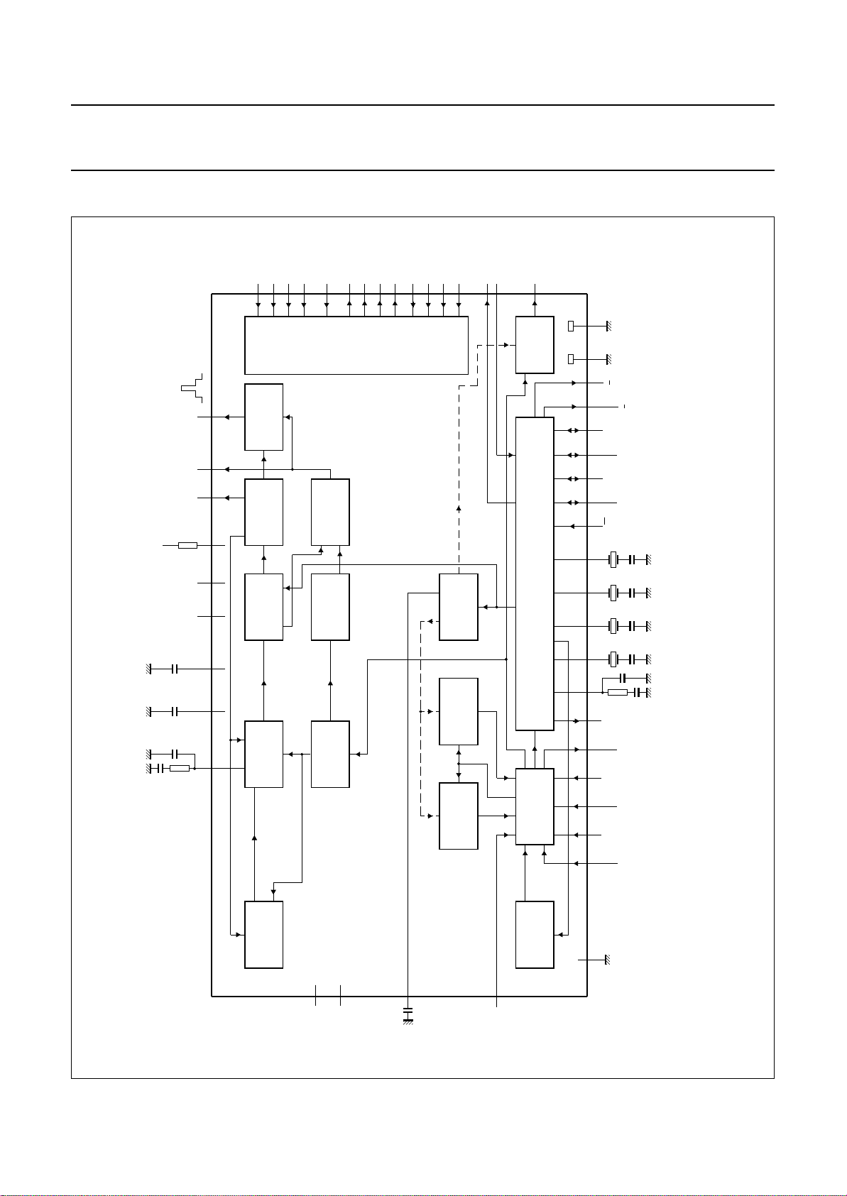
BLOCK DIAGRAM
B112G111R1
10
40
SAND
GENERATOR
SANDCASTLE
36
VOUT
39
HOUT
PULSE
SHAPER
INTB
30
BLANK1
13
CLAMP
14
RGB/YUV
DIVIDER
VERTICAL
HORIZONTAL/
SWITCH
5B6G7R8
TDA8310A
B23G22R21BLANK
BLANK2
52
IDENT
4
HUE
28
Y
49
DELAY LINE
LUMINANCE
MGD128
18 38
50 51
23
24
25
27 26
42
TDA8310A
GND1 GND3
R Y
B Y
LOGIC2
LOGIC1
COLOUR2
COLOUR1
R/W
XTAL1
41
P2
V
19
P1
V
DIG
DEC
21
BG
DEC
35
PH1LF
37
+
VCO
CONTROL
PHASE
DETECTOR
NOISE
DETECTOR
COINCIDENCE/
VERTICAL
SYNC
22, 29
i.c.
SYNC
SEPARATOR
SEPARATOR
33, 34
n.c.
FT
DEC
FILTER
TUNING
TRAP
CHROMINANCE
BANDPASS
CHROMINANCE
15
REF
32
CVBS
SW
PAL/NTSC
DECODER
INPUT
SELECTOR
Y/C
DETECTOR
AUTOMATIC
XTAL2
43
XTAL3
44
PLL XTAL4
46 45
48
O
SECAM
4716
I
CHROMA
CHROMA
917
20
31
EXT
CVBS
SW
SYST
INT
CVBS
GND2
handbook, full pagewidth
Fig.1 Block diagram.
1996 Jan 25 4

Philips Semiconductors Product specification
PAL/NTSC colour processor
for PIP applications
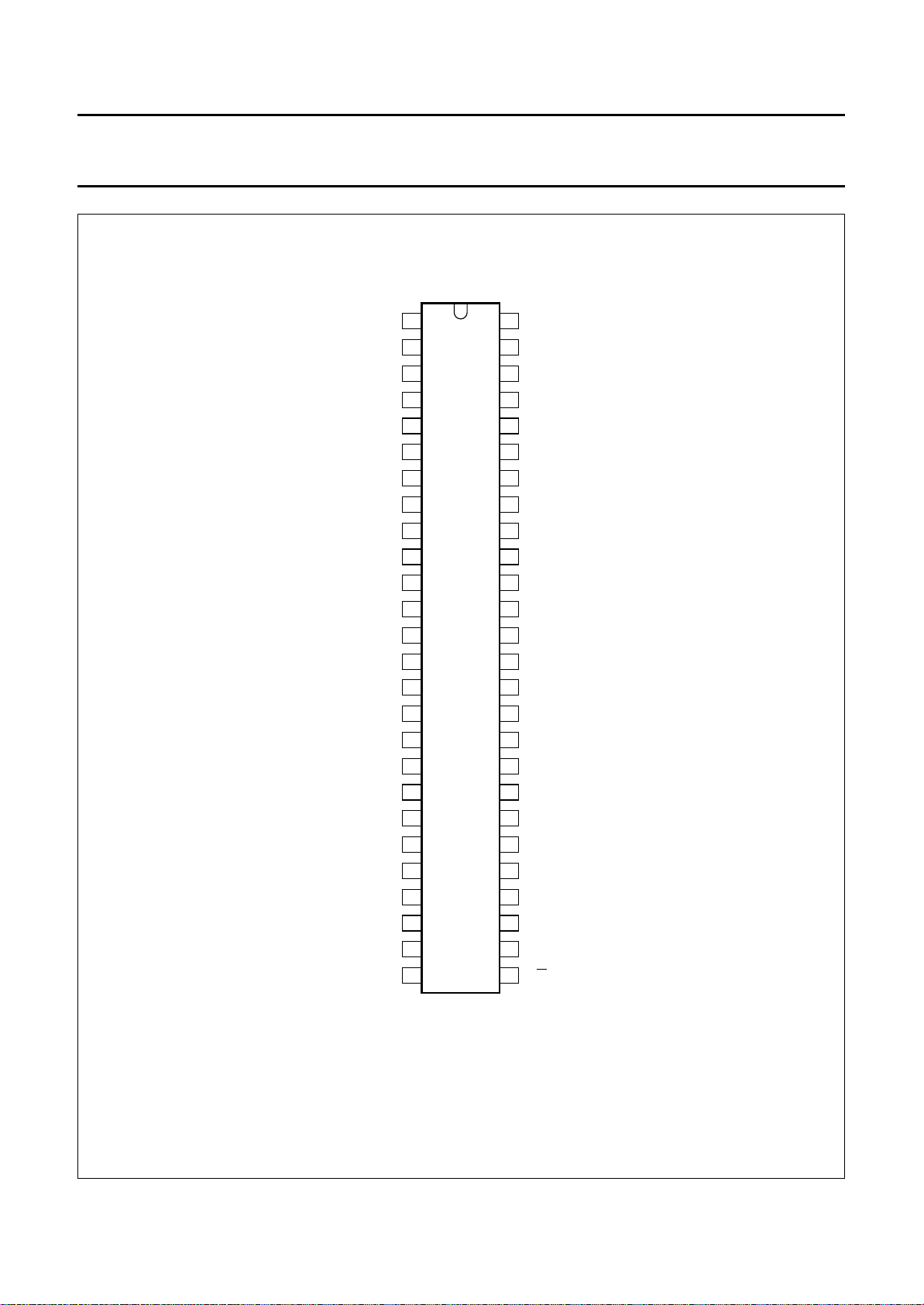
PINNING
SYMBOL PIN DESCRIPTION
R2 1 RED input 2 (PIP)
G2 2 GREEN input 2 (PIP)
B2 3 BLUE input 2 (PIP)
IDENT 4 colour standard identification output
BLANK 5 blanking output
B 6 BLUE output
G 7 GREEN output
R 8 RED output
SYST
SW
R1 10 RED input 1
G1 11 GREEN input 1
B1 12 BLUE input 1
BLANK1 13 blanking input 1
CLAMP 14 clamping pulse input
DEC
FT
CHROMA
CVBS
EXT
GND1 18 ground 1 (0 V)
V
P1
CVBS
INT
DEC
DIG
i.c. 22 internally connected (test purposes)
LOGIC2 23 crystal logic 2 input/output
LOGIC1 24 crystal logic 1 input/output
COLOUR2 25 colour system logic 2 input/output
COLOUR1 26 colour system logic 1 input/output
W 27 read/write selection input
R/
9 CVBS/system switch
15 decoupling filter tuning
16 chrominance input
I
17 external CVBS/Y input
19 supply voltage 1 (+8 V)
20 internal CVBS input
21 decoupling digital supply rail
TDA8310A
SYMBOL PIN DESCRIPTION
HUE 28 HUE control input
i.c. 29 internally connected (test purposes)
INTB 30 internal bias
GND2 31 ground 2 (0 V)
CVBS
SW
n.c. 33 not connected
n.c. 34 not connected
DEC
BG
VOUT 36 vertical sync output pulse
PH1LF 37 phase 1 loop filter
GND3 38 ground 3 (0 V)
HOUT 39 horizontal sync output pulse
SAND 40 sandcastle pulse output
V
P2
XTAL1 42 4.4336 MHz crystal
XTAL2 43 3.5820 MHz crystal for PAL-N
XTAL3 44 3.5756 MHz crystal for PAL-M
XTAL4 45 3.5795 MHz crystal for NTSC
PLL 46 PLL colour filter
CHROMA
SECAM 48 SECAM reference output
Y 49 Y output
B−Y50B−Y output
R−Y51R−Y output
BLANK2 52 blanking/insertion input 2 (PIP)
32 CVBS positive/negative modulation
control switch input
35 bandgap decoupling
41 supply voltage 2 (+8 V)
47 chrominance output for TDA8395
O
1996 Jan 25 5

Philips Semiconductors Product specification
PAL/NTSC colour processor
for PIP applications
handbook, halfpage
SYST
BLANK1
CHROMA
CVBS
CVBS
DEC
COLOUR2
COLOUR1
R2
G2
B2
IDENT
BLANK
SW
R1
G1
B1
CLAMP
DEC
FT
EXT
GND1
V
P1
INT
DIG
i.c.
LOGIC2
LOGIC1
B
G
R
I
1
2
3
4
5
6
7
8
9
10
11
12
13
TDA8310A
14
15
16
17
18
19
20
21
22
23
24
25
26
MGD127
52
51
50
49
48
47
46
45
44
43
42
41
40
39
38
37
36
35
34
33
32
31
30
29
28
27
BLANK2
R−Y
B−Y
Y
SECAM
CHROMA
PLL
XTAL4
XTAL3
XTAL2
XTAL1
V
P2
SAND
HOUT
GND3
PH1LF
VOUT
DEC
BG
n.c.
n.c.
CVBS
SW
GND2
INTB
i.c.
HUE
R/W
TDA8310A
O
1996 Jan 25 6
Fig.2 Pin configuration.
 Loading...