Philips tda8310 DATASHEETS

INTEGRATED CIRCUITS
DATA SH EET
TDA8310
PAL/NTSC colour processor for
PIP applications
Preliminary specification
File under Integrated Circuits, IC02
Philips Semiconductors
February 1995

Philips Semiconductors Preliminary specification
PAL/NTSC colour processor for
PIP applications
FEATURES
• Multistandard vision IF circuit (positive and negative
modulation)
• Video switch which automatically detects whether the
incoming signal is CVBS or Y/C
• Integrated chrominance trap and bandpass filters
(automatically calibrated)
• Integrated luminance delay line
• Automatic PAL/NTSC decoder which can decode all
standards available in the world
• Easy interfacing with the TDA8395 (SECAM decoder)
for multistandard applications
• Horizontal PLL with an alignment-free horizontal
oscillator
• Vertical count-down circuit
• RGB/YUV and fast blanking switch with 3-state output
and active clamping
• Low dissipation (560 mW)
• Small amount of peripheral components compared with
competition ICs.
TDA8310
GENERAL DESCRIPTION
The TDA8310 is an alignment-free PAL/NTSC colour
processor for Picture-in-Picture (PIP) applications. The
circuit contains a vision IF amplifier, a PAL/NTSC colour
decoder, horizontal and vertical synchronization and an
RGB/YUV switch.
As input for the colour decoder and sync processor the
demodulated IF signal can be chosen but the circuit also
has a video input which automatically detects whether the
incoming signal is CVBS or Y/C. The output signals for the
PIP processor are:
Luminance signal
Colour difference signals (U and V)
Horizontal and vertical synchronization pulses.
The RGB/YUV switch can select between two RGB or
YUV sources, e.g. between the PIP processor and the
SCART input signal.
The supply voltage for the IC is 8 V. It is available in a
52-pin SDIP package.
ORDERING INFORMATION
TYPE NUMBER
NAME DESCRIPTION VERSION
TDA8310 SDIP52 plastic shrink dual in-line package; 52 leads (600 mil) SOT247-1
PACKAGE
February 1995 2

Philips Semiconductors Preliminary specification
PAL/NTSC colour processor for
PIP applications
QUICK REFERENCE DATA
SYMBOL PARAMETER MIN. TYP. MAX. UNIT
V
P
I
P
Input voltages
V
i(rms)
V
17,20(p-p)
V
16(p-p)
V
i(p-p)
Output signals
V
o(p-p)
V
29
V
o(p-p)
V
50(p-p)
V
51(p-p)
V
39
V
36
G
v
Control voltage
V
control
supply voltage (pins 19 and 41) 7.2 8.0 8.8 V
supply current − 70 − mA
vision IF amplifier input sensitivity (RMS value) − 70 100 µV
CVBS/Y input voltage (peak-to-peak value) − 1 1.4 V
chrominance input voltage (peak-to-peak value) − 0.3 − V
RGB/YUV input signal voltage amplitude
−−1.3 V
(peak-to-peak value)
demodulated CVBS output voltage
− 2.5 − V
(peak-to-peak value)
tuner AGC control output voltage 0 − 12 V
luminance output voltage (peak-to-peak value) − 1.4 − V
(B−Y) output voltage (peak-to-peak value) 1.06 1.33 1.60 V
(R−Y) output voltage (peak-to-peak value) 0.84 1.05 1.26 V
horizontal sync pulse output voltage − 4 − V
vertical sync pulse output voltage − 4 − V
voltage gain of the RGB switches −0.5 0 +0.5 dB
control voltage for HUE 0 − 5V
TDA8310
February 1995 3

Philips Semiconductors Preliminary specification
PAL/NTSC colour processor for
PIP applications
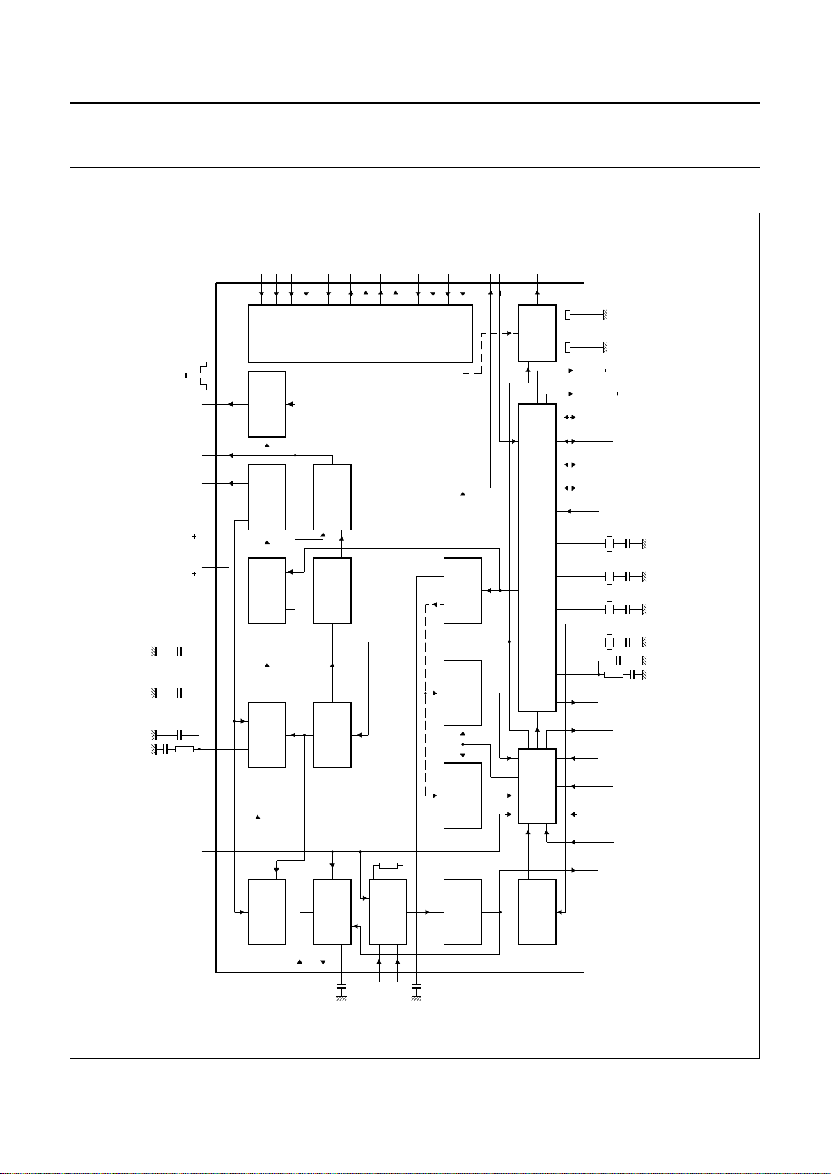
BLOCK DIAGRAM
BLANK1
13B112G111R110
40
SAND
GENERATOR
SANDCASTLE
36
VOUT
39
HOUT
PULSE
SHAPER
+
VCO
CONTROL
PHASE
DETECTOR
V
V
P1
P2
( 8 V)
( 8 V)
sw
CVBS
DIG
DEC
BG
DEC
PH1LF
19
41
21
35
37
CLAMP
14
SWITCH
RGB/YUV
DIVIDER
VERTICAL
HORIZONTAL/
SYNC
VERTICAL
SEPARATOR
SYNC
SEPARATOR
BLANK
5B6G7R8
1
TDA8310
BLANK2
B23G22R2
4
52
FILTER
TUNING
TRAP
CHROMINANCE
BANDPASS
CHROMINANCE
HUE
IDENT
REF
28
Y
49
DELAY LINE
LUMINANCE
PAL/NTSC
DECODER
INPUT
SELECTOR
MBE245
18 38
50 51
23
24
25
27 26
42
43
41
46 45
48
47
16
917
20
22
XTAL1
XTAL2
XTAL3
PLL XTAL4
GND1 GND2
R Y
B Y
LOGIC2
LOGIC1
COLOUR2
COLOUR1
R/W
0
SECAM
1
CHROMA
sw
CHROMA
SYST
EXT
CVBS
INT
CVBS
VIDEO
TDA8310
handbook, full pagewidth
Fig.1 Block diagram.
February 1995 4
NOISE
DETECTOR
COINCIDENCE/
31
ADJ
TUNER
IF AND
AGC FOR
29
AGC
TUNER
TUNER
30
AGC
C
VIF
AMPLIFIER
DEMODULATOR
34
33
IF2
IF1
15
FT
DEC
VIDEO
AMPLIFIER
Y/C
DETECTOR
AUTOMATIC

Philips Semiconductors Preliminary specification
PAL/NTSC colour processor for
PIP applications
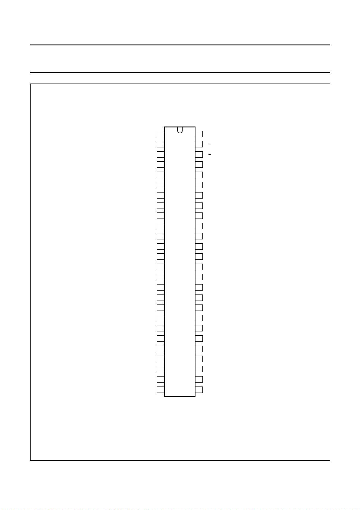
PINNING
SYMBOL PIN DESCRIPTION
R2 1 RED input 2 (PIP)
G2 2 GREEN input 2 (PIP)
B2 3 BLUE input 2 (PIP)
IDENT 4 colour standard identification output
BLANK 5 blanking output
B 6 BLUE output
G 7 GREEN output
R 8 RED output
SYST
SW
R1 10 RED input 1
G1 11 GREEN input 1
B1 12 BLUE input 1
BLANK1 13 blanking input 1
CLAMP 14 clamping pulse input
DEC
FT
CHROMA
CVBS
EXT
GND1 18 ground 1 (0 V)
V
P1
CVBS
INT
DEC
DIG
VIDEO 22 IF video output
LOGIC2 23 crystal logic 2 input/output
LOGIC1 24 crystal logic 1 input/output
COLOUR2 25 colour system logic 2 input/output
COLOUR1 26 colour system logic 1 input/output
R/W 27 read/write selection input
9 system switch
15 decoupling filter tuning
16 chrominance input
I
17 external CVBS input
19 supply voltage 1 (+8 V)
20 internal CVBS input
21 decoupling digital supply
TDA8310
SYMBOL PIN DESCRIPTION
HUE 28 HUE control input
TUNER
C
AGC
TUNER
CVBS
SW
IF1 33 IF input 1
IF2 34 IF input 2
DEC
BG
VOUT 36 vertical sync output pulse
PH1LF 37 phase 1 loop filter
GND2 38 ground 2 (0 V)
HOUT 39 horizontal sync output pulse
SAND 40 sandcastle pulse output
V
P2
XTAL1 42 4.4336 MHz crystal
XTAL2 43 3.5820 MHz crystal for PAL-N
XTAL3 44 3.5756 MHz crystal for PAL-M
XTAL4 45 3.5795 MHz crystal for NTSC
PLL 46 PLL colour filter
CHROMA
SECAM 48 SECAM reference output
Y 49 Y output
B−Y50B−Y output
R−Y51R−Y output
BLANK2 52 blanking/insertion input 2 (PIP)
29 tuner AGC output
AGC
30 AGC filter capacitor
31 tuner take-over adjustment input
ADJ
32 CVBS positive/negative modulation
control switch input
35 bandgap decoupling
41 supply voltage 2 (+8 V)
47 chrominance output for TDA8395
O
February 1995 5

Philips Semiconductors Preliminary specification
PAL/NTSC colour processor for
PIP applications
handbook, halfpage
R2
G2
B2
IDENT
BLANK
SYST
SW
R1
G1
B1
BLANK1
CLAMP
DEC
FT
CHROMA
CVBS
EXT
GND1
V
P1
CVBS
INT
DEC
DIG
VIDEO
LOGIC2
LOGIC1
COLOUR2
COLOUR1
B
G
R
I
1
2
3
4
5
6
7
8
9
10
11
12
13
14
15
16
17
18
19
20
21
22
23
24
25
26
TDA8310
MBE244
52
51
50
49
48
47
46
45
44
43
42
41
40
39
38
37
36
35
34
33
32
31
30
29
28
27
BLANK2
R Y
B Y
Y
SECAM
CHROMA
PLL
XTAL4
XTAL3
XTAL2
XTAL1
V
P2
SAND
HOUT
GND2
PH1LF
VOUT
DEC
BG
IF2
IF1
CVBS
SW
TUNER
C
AGC
TUNER
HUE
R/W
TDA8310
O
ADJ
AGC
February 1995 6
Fig.2 Pin configuration.

Philips Semiconductors Preliminary specification
PAL/NTSC colour processor for
PIP applications
FUNCTIONAL DESCRIPTION
Vision IF amplifier
The IF amplifier contains three AC-coupled control stages
with a total gain control range >60 dB. The sensitivity of
the circuit is comparable with that of modern IF-ICs. The
demodulation of the IF signal is achieved by a multiplier.
The demodulator is alignment-free and does not require
external components.
The polarity of the demodulator can be switched to make
the circuit suitable for positive and negative modulated
signals.
The AGC detector operates on top-sync or top white-level
depending on the position of the demodulator. The AGC
detector time-constant capacitor is externally connected to
facilitate flexibility of the application. During positive
modulation the time-constant of the AGC system is too
long to avoid visible variations of the signal amplitude. To
obtain an acceptable speed of the AGC system a circuit
has been included which detects whether the AGC
detector is activated every frame period. When no action
is detected during three frame periods the speed of the
system is increased.
Synchronization circuit
The sync separator is preceded by a voltage controlled
amplifier which adjusts the sync pulse amplitude to a fixed
level. The sync pulses are then fed to the slicing stage
(separator) which operates at 50% of the amplitude.
The separated sync pulses are fed to the first phase
detector and to the coincidence detector. The coincidence
detector is used to detect whether the line oscillator is
synchronized and for transmitter identification. The first
PLL has a very high static steepness, this ensures that the
phase of the picture is independent of the line frequency.
The line oscillator operates at twice the line frequency.
The oscillator network is internal. Because of the spread of
internal components an automatic adjustment circuit has
been added to the IC.
The circuit compares the oscillator frequency with that of
the crystal oscillator in the colour decoder. This results in
a free-running frequency which deviates less than 2% from
the typical value.
The horizontal output pulse is derived from the horizontal
oscillator via a pulse shaper. The pulse width of the output
pulse is 5.4 µs, the front edge of this pulse coincides with
the front edge of the sync pulse at the input.
TDA8310
The vertical output pulse is generated by a count-down
circuit. The pulse width is approximately 380 µs. Both the
horizontal and vertical pulses will always be available at
the outputs even when no input signal is available.
In addition to the horizontal and vertical sync pulse outputs
the IC has a sandcastle pulse output which contains burst
key and blanking pulses.
Integrated video filters
The circuit contains a chrominance bandpass and trap
circuit. The filters are realised by gyrator circuits that are
automatically tuned by comparing the tuning frequency
with the crystal frequency of the decoder. When a Y/C
signal is supplied to the input the chrominance trap is
automatically switched off by the Y/C detection circuit, but
it is also possible to force the filters in the CVBS or Y/C
position.
The luminance delay line is also realised by gyrator
circuits.
Colour decoder
The colour decoder contains an alignment-free crystal
oscillator, a colour killer circuit and colour difference
demodulators. The 90° phase shift for the reference signal
is achieved internally.
The colour decoder is very flexible. Together with the
SECAM decoder TDA8395 an automatic multistandard
decoder can be designed but it is also possible to use it for
one standard when only one crystal is connected to the IC.
The decoder can be forced to one of the standards via the
“forced mode” pins. The crystal pins which are not used
must be connected to the positive supply line via a 8.2 kΩ
resistor. It is also possible to connect the non-used pins
with one resistor to the positive supply line. In this event
the resistor must have a value of 8.2 kΩ divided by the
number of pins.
The chrominance output signal of the video switch is
externally available and must be used as an input signal
for the SECAM decoder.
RGB/YUV switch
The RGB/YUV switch is for switching between two RGB or
YUV video sources. The outputs of the switch can be set
to high impedance state so that other switches can be
used in parallel.
The switch is controlled via pins 13 and 52. The details of
switch control are shown in Table 5.
February 1995 7
 Loading...