

Philips TDA8303A, TDA8303 User Manual

INTEGRATED CIRCUITS
DATA SH EET
TDA8303
TDA8303A
Small signal combination IC for
black/white TV
Preliminary specification
File under Integrated Circuits, IC02
July 1992

Philips Semiconductors Preliminary specification
Small signal combination IC for black/white TV
FEATURES
• Video IF amplifier with synchronous demodulator
• Automatic gain control (AGC) detector suitable for
negative modulation
• AGC tuner
• Automatic frequency control (AFC) circuit with
sample-and-hold
• Video preamplifier
• Sound IF amplifier and demodulator
• DC volume control or separate supply for starting the
horizontal oscillator
• Audio preamplifier
• Horizontal synchronization circuit with two control loops
• Vertical synchronization (divider system) and sawtooth
generation with automatic amplitude adjustment for 50
and 60 Hz
• Transmitter identification (mute)
GENERAL DESCRIPTION
The TDA8303/TDA8303A combines all small signal
functions (except the tuner) which are required for a
monochrome television receiver. For a complete black and
white receiver only the output stages for video, sound,
horizontal and vertical deflection and a tuner have to be
added.
The TDA8303 is for applications with npn tuners and the
TDA8303A for pnp tuners.
FUNCTIONAL DESCRIPTION
Video IF amplifier, demodulator and video amplifier
Each of the three AC-coupled IF stages permits the
omission of DC feedback and possesses a control range
in excess of 20 dB. An additional advantage is the
symmetry of the amplifier which results in a less critical
application.
The IF amplifier is followed by a passive synchronous
demodulator providing a regenerated carrier signal. This is
limited by a logarithmic limiter circuit prior to its application
to the demodulator. The limiter has a very low differential
phase shift which results in good differential gain and
phase figures.
The video amplifier also contains a white spot inverter and
a noise clamp which limits interference pulses to a point
below the peak sync level. This circuit is more effective
than a noise inverter and results in an improved picture
stability, with respect to interference.
AFC-circuit
The reference signal for the AFC circuit is obtained from
the demodulator tuned circuit. In this way only one tuned
circuit needs to be applied and only one adjustment has to
be carried out. The disadvantage with this method is that
the frequency spectrum of the signal fed to the detector is
determined by the SAW filter characteristic. This spectrum
is asymmetrical with respect to the picture carrier so that
the AFC output voltage is dependent on the video signal.
To overcome this video frequency dependency of the AFC
output, the demodulator output is followed by a
sample-and-hold circuit which samples during the sync
level of the signal. This means that only the carrier signal
is available to the AFC and it will not be affected by the
video information.
At very weak input signals the drive signal of the AFC
circuit will contain substantial noise. This noise has an
asymmetrical frequency spectrum causing an offset in the
AFC output voltage. This effect can be minimized by
applying a notch in the demodulator tuned circuit. The
sample-and-hold circuit is followed by an amplifier with
high output impedance, therefore the steepness of the of
the AFC control voltage is dependent on the load
impedance.
TDA8303
TDA8303A
ORDERING INFORMATION
EXTENDED TYPE
NUMBER
TDA8303 28 DIL plastic SOT117
TDA8303A 28 DIL plastic SOT117
Note
1. SOT117-1; 1996 December 3.
July 1992 2
PINS PIN POSITION MATERIAL CODE
PACKAGE
(1)
(1)
Philips Semiconductors Preliminary specification
Small signal combination IC for black/white TV
TDA8303
TDA8303A
QUICK REFERENCE DATA
SYMBOL PARAMETER CONDITIONS MIN. TYP. MAX. UNIT
Supply
V
P
I
P
I
start
Video
V
8-9(RMS)
G
8-9
S/N signal-to-noise ratio input signal =
V
18(p-p)
Sound
V
12(RMS)
AMS AM suppression at V
THD total harmonic distortion − 0.5 − %
positive supply voltage (pin 7) 9.5 12 13.2 V
supply current (pin 7) 90 125 160 mA
start current (pin 11) note 1 − 6.5 9 mA
IF sensitivity (RMS value) at 38.9 MHz;
20 40 65 µV
note 2
IF gain control range − 74 − dB
− 57 − dB
10 mV
AFC output voltage swing
10.5 − 11.5 V
(peak-to-peak value)
AF output signal (RMS value) note 3 400 600 800 mV
= 50 mV − 58 − dB
I
Sync
V
25
I
27
V
22
required sync pulse amplitude note 4 200 −−mV
required input current during flyback pulse 0.1 − 2mA
coincidence detector output voltage
in synchronized condition − 9.7 − V
in no signal condition − 1.5 − V
V
22
V
22(p-p)
vertical feedback for DC voltage 2.9 3.3 3.7 V
vertical feedback for AC voltage
− 1.2 − V
(peak-to-peak value)
Notes to the quick reference data
1. Pin 11 has a double function. When during switch-on a current of 9 mA is supplied to this pin, it is used to start the
horizontal oscillator. The main supply can then be obtained from the horizontal deflection stage. When no current is
supplied to this pin it can be used as a volume control.
2. On set AGC.
3. The output signal is measured at ∆f = 7.5 kHz and maximum volume control.
4. The minimum value is obtained by connecting a 1.8 kΩ resistor and a 470 nF capacitor in series between the video
output and pin 25. The slicing level can be varied by changing the value of this resistor (higher resistance value
results in a larger value of the minimum sync pulse amplitude). The slicing level is independent of the video
information.
July 1992 3
Philips Semiconductors Preliminary specification
Small signal combination IC for black/white
TV
TDA8303
TDA8303A
July 1992 4
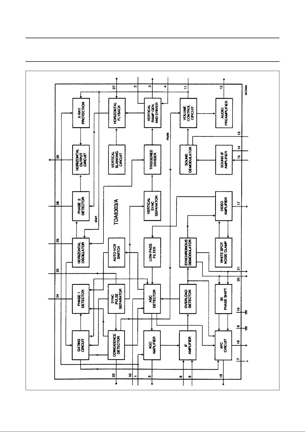
Fig.1 Block diagram

Philips Semiconductors Preliminary specification
Small signal combination IC for black/white
TV
PINNING
PIN DESCRIPTION
1 AGC take-over
2 vertical ramp generator
3 vertical drive
4 vertical feedback
5 tuner AGC
6 ground
7 supply voltage input
8 video IF input
9 video IF input
10 IF AGC
11 volume control/start horizontal oscillator
12 audio output
13 sound demodulator
14 sound IF decoupling
15 sound IF input
16 ground (for some critical parts)
17 video amplifier output
18 AFC output
19 AFC S/H, AFC switch
20 video demodulator tuned circuit
21 video demodulator tuned circuit
22 coincidence detector
23 horizontal oscillator
24 phase 1 detector
25 sync separator input
26 horizontal drive output
27 horizontal flyback input
28 phase 2 detector
TDA8303
TDA8303A
Sound circuit
The sound quality of the TDA8303/TDA8303A compared
with the predecessors has been improved at weak signal
conditions. The improvement has been achieved by the
new IF amplifier which is less sensitive for radiation from
the sound IF amplifier and by change of the ground and
supply connections in the IC. When out-of-sync condition
is detected by the coincidence detector the sound output
is muted. When no mute is required the minimum voltage
level on pin 22 should be clamped to a high level of 5 V.
At this level the gating of the AGC is switched off and the
phase 1 detector has a high output current for reliable
catching of a new transmitter.
Vertical synchronization
The TDA8303/TDA8303A embodies a synchronized
divider system for generating the vertical sawtooth at pin 2
having several advantages and features such as:
• The vertical frequency is alignment free. The divider
automatically adapts to a vertical frequency of 50 Hz or
60 Hz including automatic amplitude correction and its
operating modes offer maximum
interference/disturbance protection.
• A discriminator-window checks the accuracy of the
vertical trigger pulse. Internally clock pulses are
generated by doubling the line frequency. The divider
operates in the 60 Hz mode when the trigger pulse
appears before count 576, otherwise the 50 Hz mode
will be active.
• The divider system operates with two different reset
windows for maximum interference/disturbance
protection. The windows are activated via an up/down
counter. The counter increases its counter-value by 1 for
each time the separated vertical sync pulse appears
within the selected window, otherwise the counter value
is decreased by 1.
AGC circuit
The AGC circuit of the TDA8303/TDA8303A is a top-sync
detector. The video signal coming from the video amplifier
passes a 2nd order low-pass filter before it is compared
with an internal reference level. The comparator stage is
gated when the horizontal oscillator is synchronized with
the video signal, such that interference pulses outside the
gating time have no influence on the gain control.
July 1992 5
Modes of operation
Large search window: divider ratio between 488 and 576.
This mode is valid for the following conditions:
• Divider is looking for a new transmitter
• Divider ratio found does not comply with the narrow
window specification limits
• Up/down counter value of the divider system, operating
in the narrow window mode, drops below count 10

Philips Semiconductors Preliminary specification
Small signal combination IC for black/white TV
Narrow window mode: divider ratio between 522 and 528
(60 Hz); or 622 and 628 (50 Hz).
• The divider system switches over to narrow window
mode when the up/down counter has reached his
maximum value of 15 approved vertical sync pulses
• When the divider operates in the narrow window mode
and a vertical sync pulse is missing within the window,
the divider is reset at the end of that window and the
counter value is decreased by 1
• At a counter value below 10 the divider system switches
over to the large window mode
• The divider system also generates an anti-top-flutter
pulse which inhibits the phase 1 detector during the
vertical sync pulse. The pulse width is dependent on the
divider mode. For the large window mode the start is
generated at the reset of the divider. In the narrow
window mode the anti-top-flutter pulse starts at the
beginning of the first equalizing pulse. The
anti-top-flutter pulse ends at count 10 for the 50 Hz
mode and count 12 for the 60 Hz mode
VCR switch
An extra time constant switch in the horizontal phase
detector makes an external VCR switch redundant. The
time constant is automatically switched depending on the
signal strength of the IF input (pins 8/9) and the
coincidence detector.
When a strong signal is detected (V
circuit is synchronized the time constant of the phase
detector is optimum for VCR playback, a fast time constant
during the vertical retrace to correct head errors of the
VCR and during scan a sufficient time constant to correct
fluctuations of the horizontal sync
During weak signal and synchronized conditions the time
constant is enlarged and the phase detector is gated. This
> 2.2 mV) and the
8/9
ensures a stable display which is not disturbed by the
noise in the video signal. When the circuit is not
synchronized the time constant is fast and not gated to
ensure a short catching time.
Combination of DC volume control and start-up feature
Pin 11 of the IC can be used as a DC volume control or as
a start-up feature of the horizontal oscillator/output circuit
dependent on the application.
Volume control is achieved by connecting a 4.7 kΩ
potentiometer or a DC voltage of 0 to 3 V to pin 11. When
a current of 9 mA is supplied to pin 11 the volume control
is set to a fixed output signal level and the circuit will
generate drive pulses for the horizontal deflection and the
main supply can be derived from the deflection.
Application when external video signals require synchronization
The input to the sync separator is externally available via
pin 25. For normal application the video output signal at pin
17 is AC-coupled to the sync separator input. It is possible
to interrupt this connection and drive the sync separator
from other sources.
When external signals are applied to the sync separator
the connections between the two parts must be
interrupted. This can be achieved by connecting pin 22 to
ground, which results in the following conditions:
• AGC detector is not gated
• Mute circuit not active, sound channel remains switched
on
• Phase detector 1 has an optimum time constant for
external video sources and is not gated
TDA8303
TDA8303A
LIMITING VALUES
In accordance with the Absolute Maximum System (IEC 134)
SYMBOL PARAMETER MIN. MAX. UNIT
V
P
P
tot
T
stg
T
amb
July 1992 6
supply voltage (pin 7) − 13.2 V
total power dissipation − 2.3 W
storage temperature range −55 +150 °C
operating ambient temperature range −25 +65 °C
Philips Semiconductors Preliminary specification
Small signal combination IC for black/white TV
TDA8303
TDA8303A
CHARACTERISTICS
= 12 V;T
V
P
SYMBOL PARAMETER CONDITIONS MIN. TYP. MAX. UNIT
Supply (pin 7)
V
P
I
P
I
11
V
11
V
11
IF Amplifier (pins 8 and 9)
V
8-9(RMS)
V
8-9(RMS)
R
8-9
C
8-9
G
8-9
∆V
17
V
8-9
Video Amplifier (note 5)
V
17
V
17
V
17
V
17
V
17
Z
17
I
17
I
source
B bandwidth of demodulated output signal 5 7 − MHz
G
17
ϕ differential phase note 8 − 2 5 deg.
NL video non linearity note 9 − 25%
= 25 °C; carrier 38.9 MHz negative modulation, unless otherwise specified
amb
supply voltage range 9.5 12 13.2 V
supply current no input 90 125 160 mA
start current (pin 11) note 1 − 6.5 9 mA
start voltage horizontal oscillator 9.5 −−V
start protection level I11 = 12 mA −−16.5 V
input sensitivity (RMS value) at 38.9 MHz;
25 40 65 µV
note 2
input sensitivity (RMS value) at 45.75 MHz;
25 40 65 µV
notes 2 and 25
differential input resistance note 3 − 1300 −Ω
differential input capacitance note 3 − 5 − pF
gain control range − 74 − dB
output signal expansion for 46 dB input signal
note 4 − 1 − dB
variation
maximum input signal 100 170 − mV
zero signal output level note 6 − 5.4 − V
peak sync level 2.3 2.5 2.7 V
video output signal amplitude note 7 2.3 2.65 3.0 V
white spot threshold level − 5.7 − V
white spot insertion level − 3.8 − V
video output impedance − 25 −Ω
internal bias current of npn emitter follower
1.4 1.8 − mA
output transistor
maximum source current (pin 17) 10 −−mA
differential gain note 8 − 48%
intermodulation note 10
1.1 MHz; blue 50 60 − dB
1.1 MHz; yellow 50 60 − dB
3.3 MHz; blue 55 65 − dB
3.3 MHz; yellow 55 65 − dB
July 1992 7
 Loading...