

Philips TDA8060TS Datasheet

INTEGRATED CIRCUITS
DATA SH EET
TDA8060TS
Satellite ZERO-IF QPSK
down-converter
Product specification
Supersedes data of 1998 May 29
File under Integrated Circuits, IC02
1999 Aug 30

Philips Semiconductors Product specification
Satellite ZERO-IF QPSK down-converter TDA8060TS
FEATURES
• Direct conversion QPSK demodulation (Zero IF)
• 920 to 2200 MHz range
• On-chip loop-controlled 0 or 90° phase shifter
• Variable gain on RF input
• 60 MHz, at −1 dB, bandwidth for baseband
I and Q amplifiers
• Local oscillator output to PLL satellite or terrestrial
• 5 V supply voltage.
APPLICATIONS
• Direct Broadcasting Satellite (DBS) QPSK
demodulation
• Digital VideoBroadcasting (DVB) QPSK deSupersedes
data of 1998 May 29
modulation.
GENERAL DESCRIPTION
The direct conversion QPSK demodulator is the front-end
receiver dedicated to digital TV broadcasting, satisfying
both DVB and DBS TV standards. The 920 to 2200 MHz
wide range oscillator covers American, European and
Asian satellite bands as well as the future SMA-TV US
standard.
Accurate QPSK demodulation is ensured by the on-chip
loop-controlled phase shifter. The Zero-IF concept
discardstraditionalIFfilteringand intermediate conversion
techniques. It also simplifies the signal path.
The baseband I and Q signal bandwidth only depends, to
a certain extent, on the external filter used in the
application.
Optimum signal level is guaranteed by a gain-controlled
amplifier at the RF input. The GAIN pin sets the gain for
both I and Q channels, providing a 30 dB range.
The chip also offers a selectable internal LO prescaler
(divide-by-2) and buffer that has been designed to be
compatible with the input of a terrestrial or satellite
frequency synthesizer.
QUICK REFERENCE DATA
SYMBOL PARAMETER MIN. TYP. MAX. UNIT
V
CC
supply voltage 4.75 5.00 5.25 V
∆Φ quadrature error −−3 deg
f
V
T
osc
o(p-p)
amb
oscillator frequency 920 − 2200 MHz
output voltage (peak-to-peak value) − 0.75 − V
operating ambient temperature −20 − +85 °C
ORDERING INFORMATION
TYPE
NUMBER
NAME DESCRIPTION VERSION
PACKAGE
TDA8060TS SSOP24 plastic shrink small outline package; 24 leads; body width 5.3 mm SOT340-1
1999 Aug 30 2
This text is here in white to force landscape pages to be rotated correctly when browsing through the pdf in the Acrobat reader.This text is here in
_white to force landscape pages to be rotated correctly when browsing through the pdf in the Acrobat reader.This text is here inThis text is here in
white to force landscape pages to be rotated correctly when browsing through the pdf in the Acrobat reader. white to force landscape pages to be ...
1999 Aug 30 3
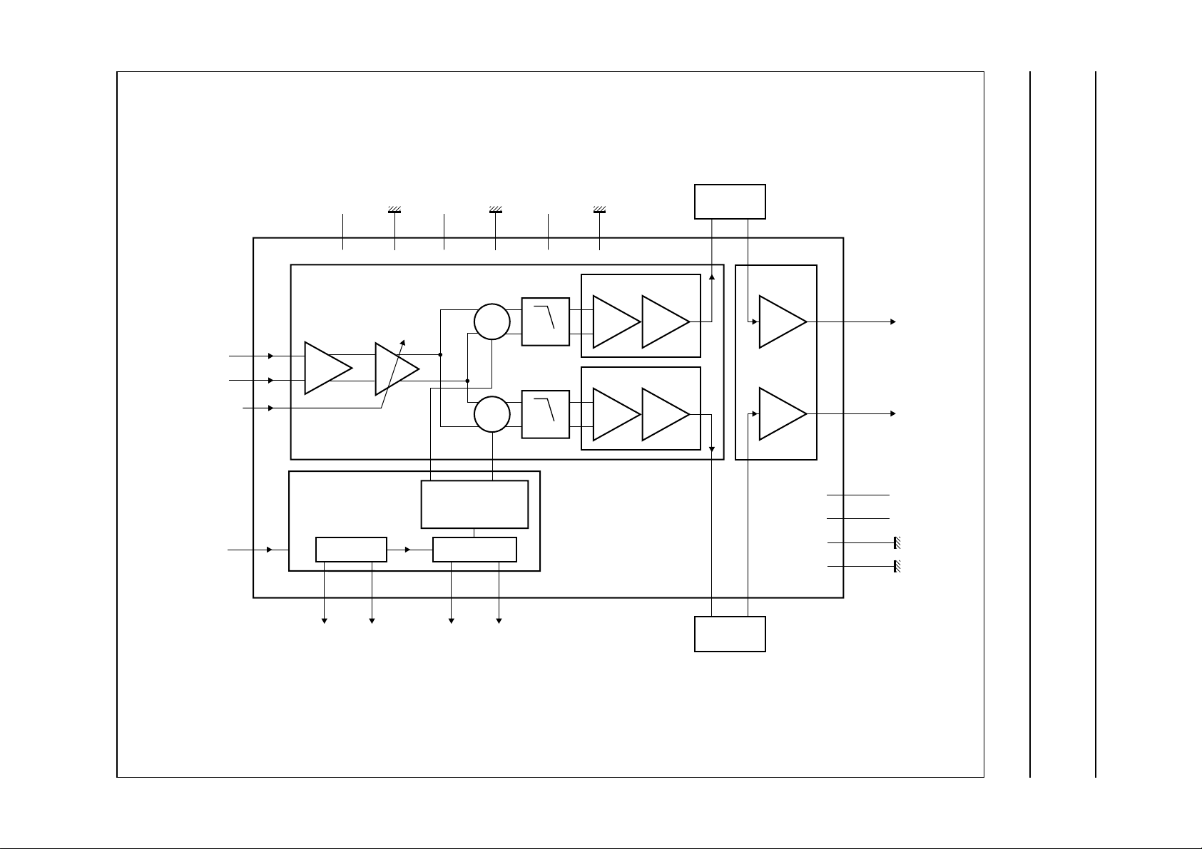
BLOCK DIAGRAM
Philips Semiconductors Product specification
Satellite ZERO-IF QPSK down-converter TDA8060TS
handbook, full pagewidth
RFA 8
RFB 7
COMGAIN 4
PEN 5
V
CC(RF)
6
LNA
QUADRATURE
GENERATOR
20
LOOUT21LOOUTC
RFGND
9
V
CC(LO1)
16
LOGND1
15
CONVERSION STAGE
×
×
STABILIZED LO
PLL AND
AMPLIFIER
OSCILLATORDIVIDE-BY-2
18
TKA17TKB
V
19
100 MHz
100 MHz
CC(LO2)
LOGND2
22
I CONVERTER
SYM
ASYM AMP
Q CONVERTER
ASYMSYM
TDA8060TS
LOW-PASS
FILTER
IOUT2IBBIN
BASEBAND
11
QOUT
LOW-PASS
FILTER
24
STAGE
AMP
13
QBBIN
12
1
IBBOUT23
QBBOUT14
V
CC(BB1)
V
CC(BB2)
BBGND13
BBGND210
MGM318
Fig.1 Block diagram.
Philips Semiconductors Product specification
Satellite ZERO-IF QPSK down-converter TDA8060TS
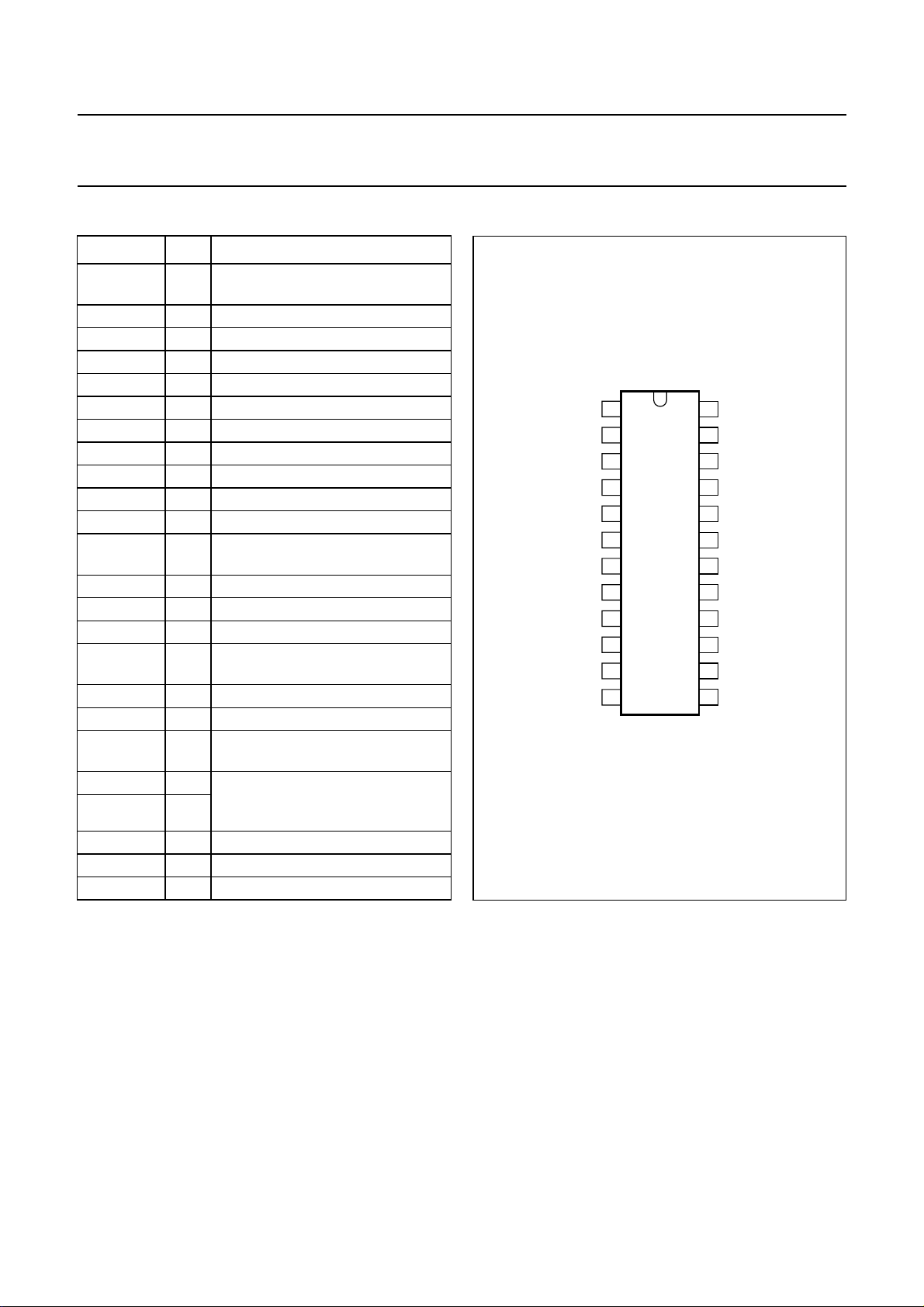
PINNING
SYMBOL PIN DESCRIPTION
V
CC(BB1)
IOUT 2 ‘I’ output from demodulator
BBGND1 3 ground 1 for baseband circuit
COMGAIN 4 RF amplifier gain control input
PEN 5 prescaler enable
V
CC(RF)
RFB 7 RF signal input B
RFA 8 RF signal input A
RFGND 9 ground for RF circuit
BBGND2 10 ground 2 for baseband circuit
QOUT 11 ‘Q’ output from demodulator
V
CC(BB2)
QBBIN 13 ‘Q’ baseband amplifier input
QBBOUT 14 ‘Q’ baseband amplifier output
LOGND1 15 ground 1 for local oscillator circuit
V
CC(LO1)
TKB 17 tank circuit input B
TKA 18 tank circuit input A
V
CC(LO2)
LOOUT 20 local oscillator output to
LOOUTC 21
LOGND2 22 ground 2 for local oscillator circuit
IBBOUT 23 ‘I’ baseband amplifier output
IBBIN 24 ‘I’ baseband amplifier input
1 supply voltage 1 for baseband
circuit (+5 V)
6 supply voltage for RF circuit (+5 V)
12 supply voltage 2 for baseband
circuit (+5 V)
16 supply voltage 1 for local oscillator
circuit (+5 V)
19 supply voltage 2 for local oscillator
circuit (+5 V)
synthesizer divided or not
according to PEN voltage
handbook, halfpage
V
COMGAIN
V
IOUT
PEN
RFB
RFA
QOUT
1
2
3
4
5
6
TDA8060TS
7
8
9
10
11
12
CC(BB1)
BBGND1
V
CC(RF)
RFGND
BBGND2
CC(BB2)
Fig.2 Pin configuration.
MGM317
24
23
22
21
20
19
18
17
16
15
14
13
IBBIN
IBBOUT
LOGND2
LOOUTC
LOOUT
V
CC(LO2)
TKA
TKB
V
CC(LO1)
LOGND1
QBBOUT
QBBIN
1999 Aug 30 4
Philips Semiconductors Product specification
Satellite ZERO-IF QPSK down-converter TDA8060TS
LIMITING VALUES
In accordance with the Absolute Maximum Rating System (IEC 134).
SYMBOL PARAMETER MIN. MAX. UNIT
V
CC
V
i(max)
t
sc(max)
T
amb
T
stg
T
j
HANDLING
Inputs and outputs are protected against electrostatic discharge in normal handling. However, to be totally safe, it is
desirable to take normal precautions appropriate to handling MOS devices.
THERMAL CHARACTERISTICS
supply voltage −0.3 +6.0 V
maximum input voltage on all pins −0.3 V
CC
V
maximum short-circuit time − 10 s
operating ambient temperature −20 +85 °C
storage temperature −55 +150 °C
junction temperature − 150 °C
SYMBOL PARAMETER CONDITIONS VALUE UNIT
R
th(j-a)
thermal resistance from junction to ambient in free air 120 K/W
DC CHARACTERISTICS
T
=25°C; VCC= 5 V; unless otherwise specified.
amb
SYMBOL PARAMETER CONDITIONS MIN. TYP. MAX. UNIT
V
CC
I
CC
supply voltage 4.75 5.00 5.25 V
supply current PEN = 5 V 63 73 83 mA
PEN=0V 607080mA
Conversion stage
V
I(RFA)
V
I(RFB)
V
O(IOUT)
V
O(QOUT)
DC input voltage on pin RFA − 0.9 − V
DC input voltage on pin RFB − 0.9 − V
DC output voltage on pin IOUT − 2.0 − V
DC output voltage on pin QOUT − 2.0 − V
Quadrature generator
V
O(LOOUT)
V
O(LOOUTC)
DC output voltage on pin LOOUT − 4.7 − V
DC output voltage on pin LOOUTC − 4.7 − V
Baseband stage
V
I(IBBIN)
V
I(QBBIN)
V
O(IBBOUT)
V
O(QBBOUT)
DC input voltage on pin IBBIN − 2.5 − V
DC input voltage on pin QBBIN − 2.5 − V
DC output voltage on pin IBBOUT − 2.5 − V
DC output voltage on pin QBBOUT − 2.5 − V
1999 Aug 30 5
 Loading...