

Philips TDA8051T-C1 Datasheet

DATA SH EET
Product specification
Supersedes data of 1998 Jan 08
File under Integrated Circuits, IC02
1999 Aug 20
INTEGRATED CIRCUITS
TDA8051
QPSK receiver
1999 Aug 20 2
Philips Semiconductors Product specification
QPSK receiver TDA8051
FEATURES
• High operating input sensitivity
• Gain controlled amplifier
• PLL controlled carrier frequency
• Low crosstalk between I and Q channel outputs
• 3-wire transmission bus
• 5 V supply voltage.
APPLICATIONS
• BPSK/QPSK demodulation.
GENERAL DESCRIPTION
This TDA8051 is a monolithic bipolar IC intended for
Quadrature Phase Shift Key (QPSK) demodulation. It
includes:
• Low noise RF and gain controlled amplifier
• Two matched mixers
• Symmetrical Voltage Controlled Oscillator (VCO) with
0to90°signal generator whosefrequency is controlled
by an integrated Phase Lock Loop (PLL) circuit.
• Two matched amplifiers for output base-band active
filtering and output buffers
The gain control is produced by output level detection
compared with an external pre-fixed reference. The PLL
consists of:
• Divide by four preamplifier
• 12-bit programmable main divider
• Crystal oscillator with 8-bit programmable reference
divider
• Phase/frequency detector combined with charge pump
to drive tuning amplifier
• 30 V output
QUICK REFERENCE DATA
All AC units are RMS values unless otherwise specified.
ORDERING INFORMATION
SYMBOL PARAMETER MIN. TYP. MAX. UNIT
V
CC
supply voltage range 4.75 5.00 5.25 V
f
I(LNA)
input carrier frequency at LNA input 44 − 130 MHz
V
I(LNA)
input level at LNA input −30 − 0 dBmV
∆Φ
I-Q
phase error between I and Q channels −±3−deg
∆G
I-Q
gain error between I and Q channels −±1−dB
α
CT(I-Q)
crosstalk between I and Q channels −−30 − dBc
IM3 3rd-order intermodulation distortion in
I and Q channels (0 dBmV at LNA_IN)
−−−45 dBc
V
o
voltage output on pin I_OUT and Q_OUT − 48 − dBmV
f
step
step at output 50 − 250 kHz
f
xtal
crystal frequency 1 − 4 MHz
T
amb
operating ambient temperature 0 − 70 °C
TYPE NUMBER
PACKAGE
NAME DESCRIPTION VERSION
TDA8751T SO32 plastic small outline package; 32 leads; body width 7.5 mm SOT287-1
1999 Aug 20 3
Philips Semiconductors Product specification
QPSK receiver TDA8051
This text is here in white to force landscape pages to be rotated correctly when browsing through the pdf in the Acrobat reader.This text is here in
_white to force landscape pagestoberotated correctly when browsing through the pdf in the Acrobat reader.This text is here inThis text is here in
white to force landscape pages to be rotated correctly when browsing through the pdf in the Acrobat reader. white to force landscape pages to be ...
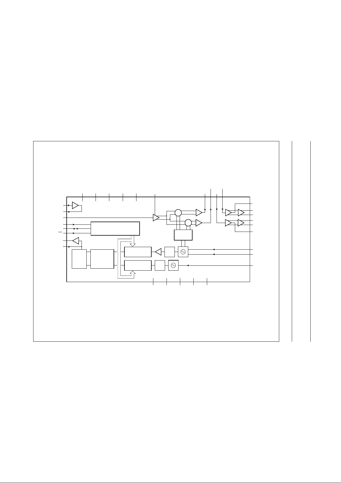
BLOCK DIAGRAM
handbook, full pagewidth
FCE112
1/2
90¡ 0¡
×
×
5
TDA8051
28
1
3
2
32
31
30
21
22
12
29 4
I_OUT1
11
I_OUT2
Q_OUT2
TKB
TKA
OSC_IN
I_OUTC
I_OUT
Q_OUTC
Q_OUT
AGC_IN
27
OUTVCC
13
DVCC
25
A3VCC
23
A2VCC
6
8
7
A1VCC
LNA_OUT
9
LNA_IN
14
CLK
15
DATA
16
EN
19
TUNE
18
CP
DEMOD_IN
Q_OUT1
Q_IN1
I_IN1
1/4
PROGRAMMABLE
MAIN DIVIDER
3-WIRE BUS TRANSCEIVER
DIGITAL
PHASE
COMPARATOR
CHARGE
1/2
PROGRAMMABLE
REF DIVIDER
17
TEST
n.c.
10
A1GND24A2GND26OUTGND20DGND
Fig.1 Block diagram.
1999 Aug 20 4
Philips Semiconductors Product specification
QPSK receiver TDA8051
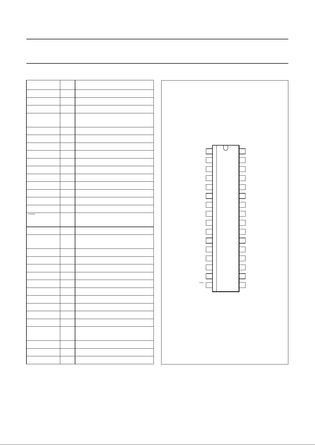
PINNING
SYMBOL PIN DESCRIPTION
I_OUT 1 I data buffered balanced output
I_OUTC 2 I data buffered balanced output
I_OUT2 3 I data filtered output
I_IN1 4 input to active filter amplifier for
I data
I_OUT1 5 I data raw output
A1VCC 6 analog supply voltage 1
DEMOD_IN 7 demodulator RF input
LNA_OUT 8 low noise amplifier RF output
LNA_IN 9 low noise amplifier RF input
A1GND 10 analog ground 1
AGC_IN 11 AGC control voltage input
OSC_IN 12 oscillator input
DVCC 13 digital supply voltage
CLK 14 3-wire bus serial control clock
DATA 15 3-wire bus serial control data
EN 16 3-wire bus serial control enable
(active LOW)
TEST 17 not connected
CP 18 charge pump output for PLL loop
filter
TUNE 19 tuning voltage output
DGND 20 digital ground
TKB 21 VCO tank circuit input
TKA 22 VCO tank circuit input
A2VCC 23 analog supply voltage 2
A2GND 24 analog ground 2
A3VCC 25 analog supply voltage 3
OUTGND 26 output amplifiers ground
OUTVCC 27 output amplifiers supply voltage
Q_OUT1 28 Q data raw output
Q_IN1 29 input to active filter amplifier for
Q data
Q_OUT2 30 Q data filtered output
Q_OUTC 31 Q data buffered balanced output
Q_OUT 32 Q data buffered balanced output
handbook, halfpage
TDA8051
FCE171
1
2
3
4
5
6
7
8
9
10
11
12
13
14
15
16
32
31
30
29
28
27
26
25
24
23
22
21
20
19
18
17
I_OUT
I_OUTC
I_OUT2
I_IN1
I_OUT1
A1VCC
DEMOD_IN
LNA_OUT
LNA_IN
A1GND
AGC_IN
OSC_IN
DVCC
CLK
Q_OUT
Q_OUTC
Q_OUT2
Q_IN1
OUTVCC
OUTGND
Q_OUT1
A3VCC
A2GND
A2VCC
TKA
TKB
DGND
TUNE
DATA
EN
CP
TEST
Fig.2 Pin configuration.
1999 Aug 20 5
Philips Semiconductors Product specification
QPSK receiver TDA8051
FUNCTIONAL DESCRIPTION
The QPSK modulated signal is applied to the input as an
asymmetrical RF signal in the bandwidth 44 to 130 MHz.
The spectrum extension to this waveform must be limited
by a band-pass filter superseding the IC.
The RF input is either the LNA input, if the level is
−30 to 0 dBmVrms, or the DEMOD input if the level is
−20 to +10 dBmVrms. The amplified RF signal is then
mixed with two clocks in quadrature to provide the
base-band demodulated In-phase (I) and Quad-phase (Q)
signals.
The VCO operates at twice the RF carrier frequency in the
bandwidth 88 - 260 MHz (one octave), therefore the
0to90° clocks are generated by a divider by 2.
The VCO frequency can be programmed by an integrated
PLL that tunes the external LC tank circuit.
The raw I and Q generated signals contain spurious
spikes, therefore each signal is passed through a third
order active low-pass filter (RC cell + Sallen-Key
structure), whose cut-off frequency is set by external
components. The filtered I and Q data signals are then
amplified to provide balanced buffer outputs.
The data sent to the PLL is loaded in bursts, framed by
signal EN. Programming clock edges, together with their
relevant data bits, are ignored until EN becomes active
(LOW). The internal latches are updated with the latest
programming data when EN returns to inactive (HIGH).
The last 14 bits only are retained within the programming
register. No check is made on the number of clock pulses
received while programming is enabled. An active clock
edge causing a shift of the data bits is generated when
EN goesHIGH while CLOCK isstillLOW. The main divider
ratio and the reference divider ratio are provided via the
serial bus (see Table 1).
LIMITING VALUES
In accordance with the Absolute Maximum Rating System (IEC 134).
HANDLING
HBM ESD: The IC pins withstand 2 kV except pin 26 (1750 V).
MM ESD: The IC pins withstand 100 V except pins 2 and 31 (75 V).
THERMAL CHARACTERISTICS
SYMBOL PARAMETER MIN. MAX. UNIT
V
CC
supply voltage −0.3 6.0 V
V
(max)
maximum voltage on all pins except pin 9 (5 V) −0.3 V
CC
V
t
sc
maximum short circuit duration on outputs − 10 s
T
stg
storage temperature −40 +150 °C
T
j(max)
maximum junction temperature − 150 °C
T
amb
operating ambient temperature 0 70 °C
V
CC(tune)
tuning voltage supply −0.3 30 V
SYMBOL PARAMETER CONDITIONS VALUE UNIT
R
th(j-a)
thermal resistance from junction to ambient in free air 65 K/W

1999 Aug 20 6
Philips Semiconductors Product specification
QPSK receiver TDA8051
CHARACTERISTICS
Measured in application circuit with the following conditions: VCC=5V; T
amb
=25°C. All AC units are RMS values,
unless otherwise specified.
SYMBOL PARAMETER CONDITIONS MIN. TYP. MAX. UNIT
Supplies
V
CCA1
analog supply voltage 4.75 5 5.25 V
I
CCA1
analog supply current − 23 − mA
V
CCA2
analog supply voltage 4.75 5 5.25 V
I
CCA2
analog supply current − 18 − mA
V
CCA3
analog supply voltage 4.75 5 5.25 V
I
CCA3
analog supply current − 29 − mA
V
cc(o)
output supply voltage 4.75 5 5.25 V
I
cc(o)
output supply current − 17 − mA
V
CCD
digital supply voltage 4.75 5 5.25 V
I
CCD
digital supply current − 13 − mA
V
CC(tune)
tuning supply voltage −−30 V
Low noise amplifier: Rs=75Ω/Ri=75Ω unless otherwise specified
V
I(DC)
DC input level internally set − 0.85 − V
V
i
input level −30 − 0 dBmV
f
i
input carrier frequency 44 − 130 MHz
R
i
input resistance − 75 −Ω
C
i
input capacitance − 2.5 − pF
R
LLNA
input return loss −−15 − dB
NF
LNA
noise figure − 711 dB
V
leak(LO)
LO leakage on pin at LNA_IN f
N × LO
= 140 − 860 MHz;
pin LNA_OUT connected to
DEMOD_IN
−−−15 dBmV
f
LO/2
=70−130 MHz;
pin LNA_OUT connected to
DEMOD_IN
−−35 −30 dBmV
G
LNA
LNA gain f = 100 MHz;
V
I(LNA)
= 0 dBmV
810−dB
V
o
output level −−20 − +10 dBmV
∆V
o
output flatness in 1 MHz bandwidth;
V
I(LNA)
= 0 dBmV
− 0.25 0.5 dB
44 to 70 MHz;
V
I(LNA)
= 0 dBmV
− 0.50 − dB
70 to 130 MHz;
V
I(LNA)
= 0 dBmV
− 1.3 1.5 dB
IM3 3rd-order intermodulation 2 carriers at +10 dBmV each −−−60 dBc
at pin LNA_IN
at 103 to 105 MHz
1999 Aug 20 7
Philips Semiconductors Product specification
QPSK receiver TDA8051
V
o(DC)
DC output level − 1.3 − V
R
o
output resistance − 75 −Ω
Quadrature demodulator: Rs=75Ω/Ri=20kΩ unless otherwise specified
V
I(DC)
DC input level internally set − 1 − V
V
i
input level −20 − +10 dBmV
f
i
input carrier frequency 44 − 130 MHz
R
i
input resistance − 75 −Ω
C
i
input capacitance − 2.5 − pF
RL
I
input Return Loss −−12 − dB
V
o(I-Q)
output level on pin I_OUT1 or
Q_OUT1
− 22 − dBmV
B
o(I-Q)
output 3 dB bandwidth LO = 200 MHz;
RF = 100 to 130 MHz
− 35 38 MHz
C/N carrier to noise ratio at
500 kHz on pin at I_OUT1 or
Q_OUT1
V
I
= −20 dBmV;
V
o(I and Q)
= 22 dBmV
− 88 − dBc/Hz
V
I
= 10 dBmV;
V
o(I and Q)
= 22 dBmV
− 93 − dBc/Hz
V
leak(LO)
LO leakage on pin
DEMOD_IN
fLO= 140 to 260 MHz;
f
LO/2
= 70 to 130 MHz
−−−15 dBmV
V
AGC(r)
AGC range fLO= 200 MHz;
fRF= 100.25 MHz at
−20 to +10 dBmV;
fBF= 250 kHz at 22 dBmV
30 −− dB
V
AGC(s)
AGC slope maximum fLO= 200 MHz;
fRF= 100.25 MHz at
−20 to +10 dBmV;
fBF= 250 kHz at 22 dBmV
− 30 − dB/V
V
AGC
gain control voltage at
AGC_IN
10% V
CCA
− 90% V
CCA
V
G
max
max. conversion gain fLO= 260 MHz;
fRF= 130.25 MHz at
−20 dBmV; V
AGC
= 4.5 V
42 −− dB
G
min
min. conversion gain fLO= 140 MHz;
fRF= 70.25 MHz at
10 dBmV V
AGC
= 0.5 V
−−12 dB
∆Φ
I-Q
phase error between I and Q
channels
fLO= 140 to 260 MHz;
fRF= 70.25 to 130.25 MHz;
fBF= 250 kHz at 22 dBmV
over specified input range
−±3−deg
∆G
I-Q
gain error between I and Q
channels
fLO= 140 to 260 MHz;
fRF= 70.25 to 130.25 MHz;
fBF= 250 kHz at 22 dBmV
over specified input range
−±1−dB
SYMBOL PARAMETER CONDITIONS MIN. TYP. MAX. UNIT
1999 Aug 20 8
Philips Semiconductors Product specification
QPSK receiver TDA8051
∆Φ
I-Q
phase error between I and Q
channels
fLO= 88 to 140 MHz;
fRF= 44.25 to 70.25 MHz;
fBF= 250 kHz at 22 dBmV
over specified input range
−±3−deg
∆G
I-Q
gain error between I and Q
channels
fLO= 88 to 140 MHz;
fRF= 44.25 to 70.25 MHz;
fBF= 250 kHz at 22 dBmV
over specified input range
−±1−dB
IM3 3rd-order intermodulation in
I and Q channels
see Fig.3 −−−45 dBc
IM2 2nd-order intermodulation in
I and Q channels
see Fig.3 −−−40 dBc
AMREJ AM rejection at I and Q
channels
guaranteed by design;
see Fig.4
−−−38 dBc
∆V
o(I/Q)
output flatness at I and Q
outputs
in 1 MHz bandwidth − 0.25 − dB
f = 40 to 70 MHz − 3 − dB
f = 70 to 130 MHz − 3 − dB
V
o(DC)
DC output level − 2.5 − V
R
o
output resistance − 400 −Ω
Output section: Rs= 400 Ω/Ri=4kΩ/R on pin I_OUT2 or Q_OUT2 = 20 kΩ unless otherwise specified
V
I(DC)
DC input voltage − 3.6 − V
V
i
input level − 22 − dBmV
R
i
input resistance − 17.5 − kΩ
C
i
input capacitance − 0.4 − pF
G
O
gain from
I-Q_IN1 to I-Q_OUT2
fBF= 1 MHz at 22 dBmV − 3.8 − dB
∆V
o(I-Q_out2)
output flatness on
pins I_OUT2 and Q_OUT2
fBF= 0 to 1.5 MHz − 0.25 − dB
f
BF
= 0 to 6 MHzat 22 dBmV
input
− 1 − dB
V
o(flt)
DC output level at filter output − 2.6 − V
R
o
output resistance f < 20 MHz − 250 −Ω
H
2
2nd harmonic fBF= 1 MHz at 48 dBmV
output
−−40 −35 dBc
H
3
3rd harmonic
f
BF
= 1 MHz at 48 dBmV
output
−−45 −40 dBc
IM3 3rd-order intermodulation at
pins I_OUTand Q_OUT
see Fig.5 −−50 −45 dBc
α
CT(I-Q)
crosstalk between I and Q
channels
f = 5 MHz; see Fig.6 −−40 −30 dBc
N
o
output noise power at
500 kHz from carrier
see Fig.7 −−56 − dBmv/Hz
G
I-Q
gain from
I-Q_IN1 to I-Q_OUT
fBF= 1 MHz at 22 dBmV
input
− 27 − dB
SYMBOL PARAMETER CONDITIONS MIN. TYP. MAX. UNIT
 Loading...