


INTEGRATED CIRCUITS
DATA SH EET
TDA8046
Multi-mode QAM demodulator
Product specification
Supersededs data of 1996 Jul 23
File under Integrated Circuits, IC02
1996 Nov 19

Philips Semiconductors Product specification
Multi-mode QAM demodulator TDA8046
CONTENTS
1 FEATURES
2 APPLICATION
3 QUICK REFERENCE DATA
4 ORDERING INFORMATION
5 BLOCK DIAGRAM
6 PINNING
7 FUNCTIONAL DESCRIPTION
7.1 Functional description of the individual blocks
7.1.1 Quadrature demodulator and half Nyquist filter
7.1.2 Equalizer
7.1.3 Lock detector
7.1.4 Carrier recovery
7.1.5 Clock recovery
7.1.6 AGC
7.1.7 Offset control
7.1.8 Loop amplifiers
7.1.9 Output formatter
7.1.10 Boundary scan
7.1.11 I2C-bus interface
7.1.12 I2C-bus write parameters
7.1.13 I2C-bus read parameters
8 LIMITING VALUES
9 THERMAL CHARACTERISTICS
10 DEMODULATOR AND HALF NYQUIST
FILTER CHARACTERISTICS
11 LOCK DETECTOR CHARACTERISTICS
12 CARRIER RECOVERY CHARACTERISTICS
13 CLOCK RECOVERY CHARACTERISTICS
14 AGC CHARACTERISTICS
15 INTEGRATED LOOP AMPLIFIERS
CHARACTERISTICS
16 CHARACTERISTICS OF DIGITAL INPUTS
AND OUTPUTS
17 PACKAGE OUTLINE
18 SOLDERING
18.1 Introduction
18.2 Reflow soldering
18.3 Wave soldering
18.4 Repairing soldered joints
19 DEFINITIONS
20 LIFE SUPPORT APPLICATIONS
21 PURCHASE OF PHILIPS I2C COMPONENTS
1996 Nov 19 2

Philips Semiconductors Product specification
Multi-mode QAM demodulator TDA8046
1 FEATURES
• Different modulation schemes: 4, 16, 32,
64 and 256-QAM
• Digital demodulator and square root raised cosine
Nyquist filter with roll-off of 15% or 20%
• High performance adaptive equalizer (no training
sequence needed)
• Digital detectors for generation of required control
voltages for carrier recovery, clock recovery and AGC
• Input format: Straight binary or 2’s complement
(up to 9 bits, TTL compatible)
• Output format: 8-bit wide bus (CMOS compatible)
2
C-bus interface to initialize and monitor the
• I
demodulator. When no I2C-bus usage; 64-QAM,
20% roll-off factor in default mode
• 5 V peripheral and analog supply voltage
• 3.3 V core supply voltage
• Boundary scan test.
• Digital-to-analog converters and operational amplifiers
allowing high flexibility for selection of the (PLL) loop
2 APPLICATION
time constants
• High maximum symbol rate (r
) of 7 Msymbols/s
s
Demodulation for digital cable TV and cable modem.
3 QUICK REFERENCE DATA
SYMBOL PARAMETER CONDITIONS MIN. TYP. MAX. UNIT
V
DDD(core)
V
DDD
V
DDA
I
DDD(core)
I
DDD
I
DDA
r
s
core supply voltage 3.00 3.30 3.60 V
digital peripheral supply voltage 4.75 5.00 5.25 V
analog supply voltage 4.75 5.00 5.25 V
core supply current V
digital peripheral supply current V
analog supply current V
DDD(core)
DDD
DDA
= 3.3 V; note 1 − 100 − mA
= 5 V; note 1 − 14 − mA
= 5 V; note 1 − 16 − mA
symbol rate −−7 Msym/s
IL implementation loss note 2 − 0.7 − dB
α Nyquist roll-off (programmable) − 15 or 20 − %
SNR
lock
signal-to-noise ratio for locking a
21 −−dB
64-QAM constellation
signal-to-noise ratio for locking a
27 −−dB
256-QAM constellation
Notes
1. The supply currents are specified for the maximum symbol frequency.
2. The implementation loss (IL) of the demodulator is defined as the distance between the measured and theoretical
BER curve as function of signal-to-noise ratio at a BER = 10
This performance depends on the chosen loop parameters (see
4 ORDERING INFORMATION
TYPE
NUMBER
NAME DESCRIPTION VERSION
TDA8046H QFP64 plastic quad flat package; 64 leads (lead length 1.95 mm);
1996 Nov 19 3
body 14 × 20 × 2.8 mm
−6
for a back-to-back measurement at the IF frequency.
Application notes
).
PACKAGE
SOT319-2

Philips Semiconductors Product specification
Multi-mode QAM demodulator TDA8046
5 BLOCK DIAGRAM
book, full pagewidth
SSD1 to 12
V
DDD1 to 9
V
TMS
TDO
TDI
TRST
TCK
TEST3
TEST2
TEST1
7, 12, 14, 17,
24, 26, 31, 34,
46, 50, 61, 64
6, 13, 16,
25, 33, 38,
45, 51, 63
44
47
48
42
SCAN TEST
BOUNDARY
43
39
40
41
C-BUS
2
I
TDA8046
CONTROL
DO0
DO7 to
27 to 30
20 to 23
FINE AGC
CONTROL
OFFSET
CONTROL
SQUARE ROOT
to DACs
internal clock for
digital processing
srs
2r
s
CLOCK GENERATOR
4r
CLKSDV
CLKOUT
32
18
OUTPUT
FORMATTER
FINE AGC
EQUALIZER
OFFSET
PHASE
DIGITAL
ROTATOR
SQUARE ROOT
RAISED COSINE
RAISED COSINE
DEMODULATOR
INPUT
TATION
REPRESEN-
CARRIER
RECOVERY
NCO
CONTROL
CLOCK
RECOVERY
AGC
COARSE
ref
ref3
I
V
DAC
ref1Iref2Iref3
I
BIAS
GENERATOR
ref
ANALOG SECTION
V
ref
ref2
I
V
DAC
ref
ref1
I
V
DAC
565552
5857
59
60
5453
MGG198
CARREC
V
CARTC
V
BIAS
I
CLKREC
V
CLKTC
V
SSA
V
DDA
V
AGC
V
AGCTC
V
Fig.1 Block diagram.
1996 Nov 19 4
15
35
36
37
SCL
SDA
62
A0
CLK
CLKADC
1 to 5,
8 to 11
DIN0
to
DIN8
49
PRESET
19
CLKT

Philips Semiconductors Product specification
Multi-mode QAM demodulator TDA8046
6 PINNING
SYMBOL PIN I/O DESCRIPTION
DIN0 1 I digital input bit 0 (LSB)
DIN1 2 I digital input bit 1
DIN2 3 I digital input bit 2
DIN3 4 I digital input bit 3
DIN4 5 I digital input bit 4
V
DDD1
V
SSD1
DIN5 8 I digital input bit 5
DIN6 9 I digital input bit 6
DIN7 10 I digital input bit 7
DIN8 11 I digital input bit 8 (MSB)
V
SSD2
V
DDD2
V
SSD3
CLKADC 15 O clock output to ADC (4 × r
V
DDD3
V
SSD4
CLKSDV 18 O clock symbol data valid output
CLKT 19 I for test purpose only
DO7 20 O parallel data output (bit 7)
DO6 21 O parallel data output (bit 6)
DO5 22 O parallel data output (bit 5)
DO4 23 O parallel data output (bit 4)
V
SSD5
V
DDD4
V
SSD6
DO3 27 O parallel data output (bit 3)
DO2 28 O parallel data output (bit 2)
DO1 29 O parallel data output (bit 1)
DO0 30 O parallel data output (bit 0)
V
SSD7
CLKOUT 32 I output formatter clock output
V
DDD5
V
SSD8
SCL 35 I serial clock input (I
SDA 36 I/O serial data input/output (I
A0 37 I hardware address input (I
V
DDD6
TEST3 39 I test input 3 (normally connected to ground)
TEST2 40 I test input 2 (normally connected to ground)
6 supply digital peripheral supply voltage 1 (+5 V)
7 supply digital ground 1; for input peripheral and core
12 supply digital ground 2; for core and clock buffers
13 supply digital supply voltage 2; for core and clock buffers (+3.3 V)
14 supply digital peripheral ground 3
)
s
16 supply digital peripheral supply voltage 3 (+5 V)
17 supply digital ground 4; for core
24 supply digital peripheral ground 5
25 supply digital peripheral supply voltage 4 (+5 V)
26 supply digital ground 6; for core
31 supply digital peripheral ground 7
33 supply digital peripheral supply voltage 5 (+5 V)
34 supply digital peripheral ground 8
2
C-bus)
2
C-bus)
2
C-bus)
38 supply digital peripheral supply voltage 6 (+5 V)
1996 Nov 19 5

Philips Semiconductors Product specification
Multi-mode QAM demodulator TDA8046
SYMBOL PIN I/O DESCRIPTION
TEST1 41 I test input 1 input (normally connected to ground)
TRST 42 I optional asynchronous reset input
TCK 43 I dedicated test clock input
TMS 44 I input control signal
V
DDD7
V
SSD9
TDO 47 O serial test data output
TDI 48 I serial test data input
PRESET 49 I set device into default mode input
V
SSD10
V
DDD8
I
BIAS
V
AGCTC
V
AGC
V
CARTC
V
CARREC
V
CLKTC
V
CLKREC
V
SSA
V
DDA
V
SSD11
CLK 62 I clock input (4 × r
V
DDD9
V
SSD12
45 supply digital supply voltage 7; for core (+3.3 V)
46 supply digital ground 9; for core
50 supply digital ground 10; for the digital section of the analog block
51 supply digital supply voltage 8; for the digital section of the analog block (+5 V)
52 I input bias current for DACs
53 O inverted operational amplifier input voltage for loop filtering
54 O analog output voltage for AGC
55 O inverted operational amplifier input voltage for carrier recovery loop
filtering
56 O analog output voltage for carrier recovery
57 O inverted operational amplifier input voltage for clock recovery loop
filtering
58 O analog output voltage for clock recovery
59 supply analog ground
60 supply analog supply voltage (+5 V)
61 supply digital ground 11; for clock
)
s
63 supply digital supply voltage 9; for clock
64 supply digital peripheral ground 12
1996 Nov 19 6

Philips Semiconductors Product specification
Multi-mode QAM demodulator TDA8046
DDD9
handbook, full pagewidth
DIN0
DIN1
DIN2
DIN3
DIN4
V
DDD1
V
SSD1
DIN5
DIN6
DIN7
DIN8
V
SSD2
V
DDD2
V
SSD3
CLKADC
V
DDD3
V
SSD4
CLKSDV
CLKT
SSD12
V
V
64
63
1
2
3
4
5
6
7
8
9
10
11
12
13
14
15
16
17
18
19
20
21
CLK
62
22
SSD11
V
61
23
DDA
V
60
TDA8046
24
SSA
V
59
25
CLKREC
V
V
58
57
26
27
CLKTC
V
56
28
CARREC
CARTC
V
55
29
AGC
V
54
30
AGCTC
V
53
31
BIAS
I
52
32
51
50
49
48
47
46
45
44
43
42
41
40
39
38
37
36
35
34
33
MGG197
V
DDD8
V
SSD10
PRESET
TDI
TDO
V
SSD9
V
DDD7
TMS
TCK
TRST
TEST1
TEST2
TEST3
V
DDD6
A0
SDA
SCL
V
SSD8
V
DDD5
1996 Nov 19 7
DO7
DO6
DO5
DO4
SSD5
V
Fig.2 Pin configuration.
DDD4
V
SSD6
V
DO3
DO2
DO1
DO0
SSD7
V
CLKOUT

Philips Semiconductors Product specification
Multi-mode QAM demodulator TDA8046
7 FUNCTIONAL DESCRIPTION
Figure 3 shows the application of the TDA8046
multi-mode QAM demodulator. The frequency of the IF
signal (IF
) is down converted to a frequency that
QAM
equals the symbol rate (rs) by a mixer which is driven from
a local oscillator with a frequency of f
CAR=fIF+rs
.
After low pass filtering this baseband signal is applied to an
external 8 or 9-bit ADC.
For 256-QAM, a 9-bit ADC is preferred, for the other
modes an 8-bit ADC is sufficient.
The multi-mode QAM demodulator has digital detectors for
AGC, carrier recovery and clock recovery. The on-chip
DACs translate the detector values to analog control
handbook, full pagewidth
IF
RF
signal
SAWTUNER
QAM
currents which are then integrated by a loop filter.
To perform this loop filtering, an operational amplifier is
integrated after each DAC.
The carrier recovery consists of a two-loop system.
The outer loop is shown in Fig.3, and controls both phase
and frequency at a low speed. The inner loop controls the
carrier phase at a high speed (wide loop bandwidth).
The AGC also consists of two loops; the outer loop is the
coarse AGC and one inner loop is the fine AGC.
The recovered symbols are converted into bits according
to a demapping scheme and represented at the output in
an 8-bit parallel output format. The QAM demodulator can
2
be initialized and monitored by the I
8 or 9 bits
f
clk
f
CAR
= fIF + r
LPF ADC
s
C-bus interface.
clock recovery
carrier recovery
AGC
TDA8046
2
I
C-BUS
Fig.3 Application with multi-mode QAM demodulator.
DO7 to DO0
CLKOUT
CLKSDV
MGG167
1996 Nov 19 8

Philips Semiconductors Product specification
Multi-mode QAM demodulator TDA8046
7.1 Functional description of the individual blocks
The functional block diagram of the multi-mode QAM
demodulator is illustrated in Fig.1. This section describes
the individual blocks in the demodulator. After adaptation
for the used input format (2’s complement or binary), the
input signal is demodulated in the I and Q baseband
signals which are applied to the inputs of the half-Nyquist
filter (equals square root raised cosine). To avoid
overloading of the ADC, an AGC detector is placed after
the adaptation for the input format. The control value for
the clock recovery is generated after half Nyquist filtering.
The echoes created in the cable network are reduced
significantly in the equalizer.
The equalizer produces a ‘clean’ constellation diagram
from which the information for the carrier recovery is
derived. This constellation is also applied to the output
formatter which demaps the transmitted symbols in
corresponding bits. The carrier recovery and lock
detection functions are based on the equalizer output.
The output of the equalizer is applied to an output
formatter, which translates the symbol bits to a FEC input
format. The digital outputs of the clock recovery, AGC, and
carrier recovery section are converted into currents which
are integrated by the loop filters.
To make these loop filters active, operational amplifiers
are integrated on the chip.
The TDA8046 can handle five different digital modulation
schemes; 4, 16, 32, 64 and 256-QAM. These schemes
2
are selectable via the I
7.1.1 Q
UADRATURE DEMODULATOR AND HALF NYQUIST
FILTER
C-bus interface.
Quadrature demodulation is accomplished after selection
of the appropriate input format via the I2C-bus.
The in-phase and quadrature components are both
applied to a half Nyquist filter. In default mode, this filter
gives a 20% roll-off half Nyquist shaping. The basic
schematic of the quadrature demodulator followed by the
half Nyquist filter is shown in Fig.4. The signs of the
multiplication factors in the Q-branch can be inverted
(I2C-bus bit INVD).
When using an 8-bit ADC the LSB of the 9-bit input word
should be connected to the positive supply (V
DDD
).
This ensures a symmetrical 2’s complement
representation which can be multiplied by −1 in a correct
(2’s complement) way. The overall transfer function of the
square root raised cosine filters is shown in Figs 5 and 6.
For characteristics see Chapter 10.
handbook, full pagewidth
9
COMPLEMENT
BINARY OR
TWO's
I2C-BUS
+1, 0, −1, 0
0, −1, 0, +1
I2C-BUS
DIN8
to
DIN0
Fig.4 Schematic diagram of the quadrature demodulator and half Nyquist filter.
1996 Nov 19 9
9
I
9
Q
2
I
C-BUS
HALF NYQUIST
FILTER
HALF NYQUIST
FILTER
2
C-BUS
I
MGG168

Philips Semiconductors Product specification
Multi-mode QAM demodulator TDA8046
handbook, full pagewidth
5
0
−5
relative
gain
(dB)
−15
−25
−35
−45
−55
010.25 0.5 0.75 1.751.51.25
relative frequency
Fig.5 Half Nyquist receiver filter transfer function (20% roll-off).
MBG987
f )
(
2
r
s
handbook, full pagewidth
0
relative
gain
(dB)
−10
−20
−30
−40
−50
0 0.5 1 1.50.25 0.75 1.25 1.75
Fig.6 Half Nyquist receiver filter transfer function (15% roll-off).
relative frequency
MGG169
f )
(
2
r
s
1996 Nov 19 10
Philips Semiconductors Product specification
Multi-mode QAM demodulator TDA8046
7.1.2 EQUALIZER
This function is realized with a T spaced 12 or 14 taps
(selected via the I2C-bus) adaptive filter with a feedback
part. The equaliser is based on a Decision Feedback
Equalizer (DFE) structure with Least Mean Square (LMS)
coefficient updating algorithm. No training sequence is
required. The block schematic of the total equalizer is
shown in Fig.8. The main tap of the equalizer is adjustable
for fine AGC function (6 dB AGC range). The settings of
the equalizer taps can be read via the I2C-bus. If the
2
equalizer diverges, an alarm bit is set (I
C-bus bit ALEQ)
and an automatic reset of the taps can be performed
(I2C-bus bit EAR).
To improve acquisition time, the convergence steps of the
FFE/DFE parts of the equalizer are programmable via the
I2C-bus. When the system locks, the steps are
automatically modified for optimum performances.
Besides reading the equalizer tap values, the main tap of
the equalizer can also be programmed. After setting the
main tap, the other coefficients can be set to zero.
The equalizer settings can also be frozen via the I2C-bus.
The equalizer has been proven to work correctly under bad
channel conditions as indicated in Table 1. It is guaranteed
that all loops (including equalizer) converge at a SNR of
21 dB for a 64-QAM modulation format and 27 dB for a
256-QAM modulation format.
Table 1 Channel echo profile
DELAY AMPLITUDE PHASE
3
⁄8× T
1
1
2 × T
5
4
7
6
⁄8× T
⁄8× T
⁄8× T
sym
sym
sym
sym
sym
0.08 130°
0.20 60°
0.05 310°
0.10 200°
0.03 200°
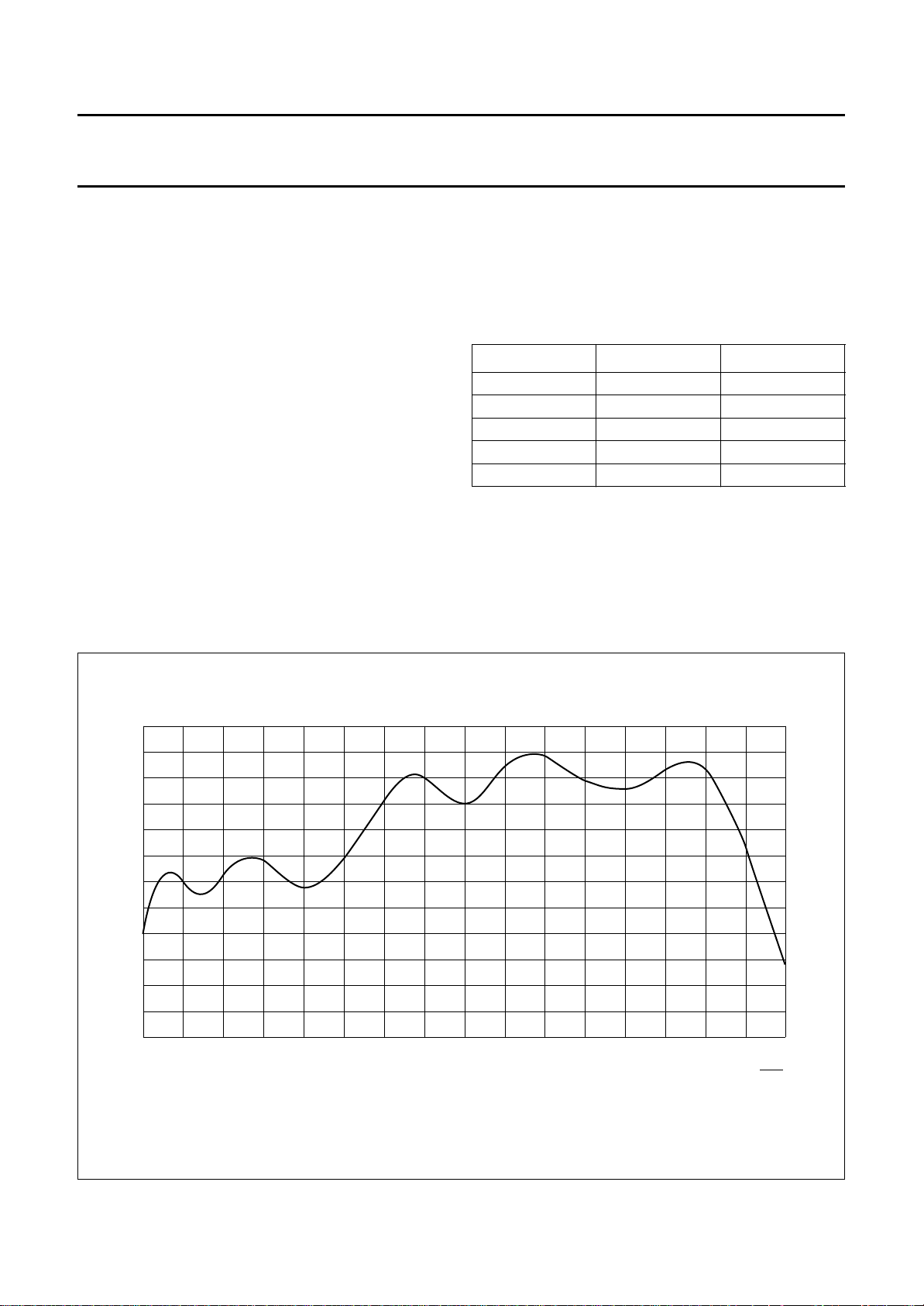
Figure 7 represents the QAM spectrum seen by the
equalizer. It corresponds (in the frequency domain) to the
multiplication of a full nyquist spectrum by the impulse
response of the channel specified in Table 1.
handbook, full pagewidth
1
relative
gain
(dB)
−1
−3
−5
−7
−9
−11
−0.5 0.5
−0.375 0.375−0.125 0.125−0.25 0.250
Fig.7 QAM spectrum with echo profile as seen by the equalizer.
relative frequency
MGD636
f )
(
r
s
1996 Nov 19 11

Philips Semiconductors Product specification
Multi-mode QAM demodulator TDA8046
handbook, full pagewidth
input
FEED
FORWARD
EQUALIZER
TAPS CALCULATION
−
Fig.8 DFE equalizer structure.
7.1.3 LOCK DETECTOR
The lock detector indicates whether all algorithms in the
demodulator are converged or not. For a symbol error rate
(at the input of the demodulator) smaller than 2 × 10⁻², the
detector will give the indication ‘LOCK’ (I2C-bus bit
LK = 1). For larger symbol error rates, the detector will
generate the ‘UNLOCK’ signal (I2C-bus bit LK = 0).
It should ne noted that this ‘UNLOCK’ signal is generated
before any other part of the demodulator loses lock.
The lock detector is part of the carrier recovery loop, see
Fig.9. The Lock Detector Threshold (LDT) can be changed
2
with the help of the I
C-bus. The estimation algorithm used
in the lock detector also provides information about the
SER ratio which can be read out via the I2C-bus interface.
For characteristics see Chapter 11.
7.1.4 C
ARRIER RECOVERY
The carrier recovery detector consists of a
Phase-Frequency Detector (PFD) and Phase Detector
(PD). Depending on the mode of operation, the carrier
recovery is switched either between the phase frequency
(no lock) or the phase detector (lock). The carrier recovery
consists of the following two loops:
DECISION
FEEDBACK
EQUALIZER
TAPS CALCULATION
decision
+
MGG170
output
1. The outer loop; this loop controls the phase and
frequency of the incoming QAM signal at the IF
frequency in such a way that the constellation is
optimally positioned for detection.
2. The inner loop; the bandwidth of this loop can be large
and can therefore reduce the influence of large
bandwidth phase noise.
A fully digital carrier recovery function is also possible and
can be selected via the I
2
C-bus. Should this configuration
be used, then the external components of the loop filter will
not have to be implemented.
Four different maximum DAC output currents can be
selected via the I2C-bus. The output currents of the DAC
are defined in such a way that a VCO with a behaviour as
shown in Fig.9 can be connected directly to the output of
the integrated operational amplifier. Should the VCO slope
be negative then the sign of the current can be inverted by
the I2C-bus. Figure 10 defines the DAC output currents.
For characteristics see Chapter 12.
1996 Nov 19 12
Philips Semiconductors Product specification
Multi-mode QAM demodulator TDA8046
handbook, full pagewidth
IF
QAM
VCO
LPF
ADC
external
DAC
I
CAR
V
I2C-BUS
DEMODULATION
AND
FILTERING
I2C-BUS
ref
DIGITAL
INNER LOOP
r
EQUALIZER
I
s
ref1
lock
LOCK
PHASE
FREQUENCY
DETECTOR
PHASE
DETECTOR
lock
Fig.9 Schematic diagram of the carrier recovery.
I2C-BUS
I2C-BUS
0
2
I
C-BUS
MGG171
1996 Nov 19 13

Philips Semiconductors Product specification
Multi-mode QAM demodulator TDA8046
handbook, full pagewidth
CARI = 1
I
= positive output current.
pos
I
= negative output current.
neg
I
–()
posIneg
I
=
------------------------------ -
O
∆ I
-------------------------------- -
O
2
I
+()
posIneg
–()
I
posIneg
I
CAR
DAC output
current
f
VCO
CARI = 0
1
/
I
CAR
2
V
CARREC
MGG180
−1/
−I
I
2
CAR
digital input
CAR
100×=
Fig.10 Definition of the DAC currents and the expected frequency behaviour of the VCO.
1996 Nov 19 14
 Loading...