

Philips TDA8043H, TDA8043AH Datasheet
DATA SH EET
Product specification
Supersedes data of 1997 Nov 07
File under Integrated Circuits, IC02
1998 Feb 13
INTEGRATED CIRCUITS
TDA8043
Satellite Demodulator and Decoder
(SDD)

1998 Feb 13 2
Philips Semiconductors Product specification
Satellite Demodulator and Decoder (SDD) TDA8043
FEATURES
• One-chip Digital Video Broadcasting (DVB) compliant
demodulator and concatenated Viterbi/Reed-Solomon
decoder with de-interleaver and de-randomizer
• 3.3 V supply voltage (up to 5 V allowed)
• Internal clock divider
• On-chip crystal oscillator
• QPSK/BPSK demodulator:
– Interpolator to handle variable symbol rates without
an external anti-aliasing filter
– On-chip Automatic Gain Control (AGC) of the analog
input I and Q baseband signals or tuner AGC control
– Two on-chip matched Analog-to-Digital Converters
(ADCs; 7 bits)
– Square-Root Raised-Cosine Nyquist filter with
programmable roll-off factor
– High maximum symbol frequency: 32 Msymbols/s
– Can be used at low channel Es/No
(Symbol energy-to-noise ratio)
– Internal carrier recovery, clock recovery and AGC
loops with programmable loop filters
– Two carrier recovery loops enabling phase tracking of
the incoming symbols
– Different modulation schemes: Quadrature Phase
Shift Keying (QPSK) and Binary-Phase Shift Keying
(BPSK)
– Signal-to-noise ratio (S/N) estimation
– External indication of demodulator lock.
• Viterbi decoder:
– Rate
1
⁄2convolutional code based
– Constraint length K = 7 with G1= 171
oct
and
G2= 133
oct
– Supported puncturing code rates:1⁄2,2⁄3,3⁄4,4⁄5,5⁄6,
6
⁄7,7⁄8and8⁄
9
– 4 bits ‘soft decision’ inputs for both I and Q
– Truncation length: 144
– Automatic synchronization to correct puncturing rate
and spectral inversion
– Channel Bit Error Rate (BER) estimation from
10−2to 10
−8
– External indication of Viterbi synchronization lock
– Differential decoding supported.
• Reed-Solomon (RS) decoder:
– (204, 188 and T = 8) Reed Solomon code
– Automatic (I
2
C-bus configurable) synchronization of
bytes, transport packets and frames
– Internal convolutional de-interleaving (I = 12; using
internal memory)
– De-randomizer based on Pseudo Random Binary
Sequence (PRBS)
– External indication of RS decoder sync lock
– External indication of uncorrectable errors (transport
error indicator is set)
– Indication of the number of lost blocks
– Indication of the number of corrected blocks/bytes.
• I2C-bus interface:
–I2C-bus interface initializes and monitors the
demodulator and Forward Error Correction (FEC)
decoder with standby mode; when no I2C-bus is
used, default mode is defined
– 4-bit I/O expander for flexible access to and from the
I2C-bus
–I2C-bus configurable interrupt pin
– Standby mode for reduced power consumption.
• Package: QFP100
• Boundary scan test.
APPLICATIONS
• Demodulation and FEC for digital satellite TV.

1998 Feb 13 3
Philips Semiconductors Product specification
Satellite Demodulator and Decoder (SDD) TDA8043
GENERAL DESCRIPTION
This document specifies a DVB compliant demodulator
and forward error correction decoder IC for reception of
QPSK and BPSK modulated signals for satellite
applications.
The TDA8043 can handle variable symbol rates without
adapting the analog filters within the tuner. Typical
applications for this device are:
• Single Carrier Per Channel (SCPC): two or more
QPSK or BPSK modulated signals in a single satellite
channel (transponder)
• Multi-Carrier Per Channel (MCPC): one QPSK or
BPSK modulated signal in a single satellite channel
(transponder)
• Simul-cast: QPSK or BPSK modulated signal together
with a Frequency Modulated (FM) signal in a single
satellite channel.
The SDD requires the analog in-phase (I) and quadrature
(Q) components as an input and provides 8-bit wide
MPEG2 transport packet data at the output. The outputs of
the SDD can be directly connected to a descrambler
(SAA7206) or a demultiplexer (SAA7205).
For evaluation purposes, the output can also be used to
monitor internal data, for example I/Q after demodulation.
The SDD requires a single clock frequency which is
independent of the received symbol rate, providing the
clock frequency is slightly higher than twice the highest
symbol frequency.
All loops to recover the data from the received symbols are
internal. No external loop components are required. Loop
parameters for the clock, carrier recovery and AGC can be
controlled via the I
2
C-bus.
The Forward Error Correction (FEC) unit has a built-in
state machine to achieve lock without knowing the system
parameters (depuncturing rate, spectral inversion, etc.).
Once lock is achieved, all necessary parameters can be
read via the I2C-bus. By programming these parameters in
advance lock can be achieved more quickly.
The SDD can be controlled and monitored via the I2C-bus.
An I2C-bus default mode is specified which makes it
possible to use the device by software control. A 4-bit
bidirectional I/O expander and an interrupt line are
available. By sending an interrupt signal, the SDD can
inform the microcontroller of its internal status (lock).
ORDERING INFORMATION
TYPE
NUMBER
PACKAGE
NAME DESCRIPTION VERSION
TDA8043H QFP100 plastic quad flat package; 100 leads (lead length 1.95 mm);
body 14 × 20 × 2.8 mm
SOT317-2
1998 Feb 13 4
Philips Semiconductors Product specification
Satellite Demodulator and Decoder (SDD) TDA8043
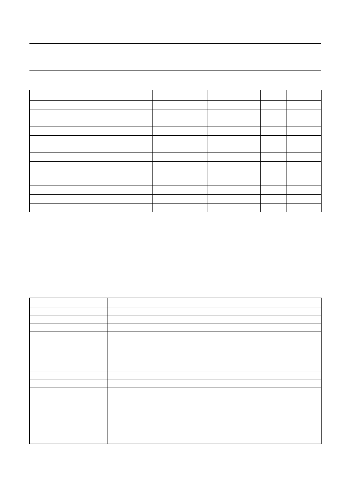
QUICK REFERENCE DATA
Notes
1. These values are specified for a symbol rate of 27.5 Msymbols/s, a puncturing rate of
3
⁄4 and a clock frequency of
65 MHz.
2. A range from 3 to 32 Msymbols/s can be achieved with one SAW filter. By using an internal clock divider and
reducing the external SAW filter bandwidth, symbol rates down to 0.5 Msymbols/s can be achieved by using a
65 MHz crystal clock.
3. This data was measured in a laboratory environment at a symbol rate of 27.5 Msymbols/s, a clock frequency of
65 MHz, a signal-to-noise ratio of 4.5 dB and including a tuner.
PINNING
SYMBOL PARAMETER CONDITIONS MIN. TYP. MAX. UNIT
V
DDA
analog supply voltage 3.0 3.3 3.6 V
V
DDD
digital supply voltage 3.0 3.3 3.6 V
I
DD(tot)
total supply current V
DDD
= 3.3 V; note 1 − 390 − mA
f
clk
clock frequency −−65 MHz
r
s
symbol rate note 2 0.5 − 32 Msymbols/s
α nyquist roll-off (selectable) − 35 or 50 − %
IL implementation loss note 3 − 0.3 − dB
S/N signal-to-noise ratio for locking
the SDD
QPSK mode; note 1 2 −−dB
P
tot
total power dissipation T
amb
=70°C; note 1 − 1285 1650 mW
T
stg
IC storage temperature −55 − +150 °C
T
amb
operating ambient temperature 0 − 70 °C
T
j
operating junction temperature T
amb
=70°C −−125 °C
SYMBOL PIN I/O DESCRIPTION
I2 1 I digital I-input bit 2 (ADC bypass); note 1
I3 2 I digital I-input bit 3 (ADC bypass); note 1
V
SSD1
3 − digital ground 1
n.c. 4 − not connected
n.c. 5 − not connected
I4 6 I digital I-input bit 4 (ADC bypass); note 1
I5 7 I digital I-input bit 5 (ADC bypass); note 1
I6 8 I digital I-input bit 6 (ADC bypass: MSB); note 1
Q0 9 I digital Q-input bit 0 (ADC bypass: LSB); note 1
V
DDD1
10 − digital supply voltage 1
Q1 11 I digital Q-input bit 1 (ADC bypass); note 1
Q2 12 I digital Q-input bit 2 (ADC bypass); note 1
Q3 13 I digital Q-input bit 3 (ADC bypass); note 1
Q4 14 I digital Q-input bit 4 (ADC bypass); note 1
V
SSD2
15 − digital ground 2
Q5 16 I digital Q-input bit 5 (ADC bypass); note 1
Q6 17 I digital Q-input bit 6 (ADC bypass: MSB); note 1
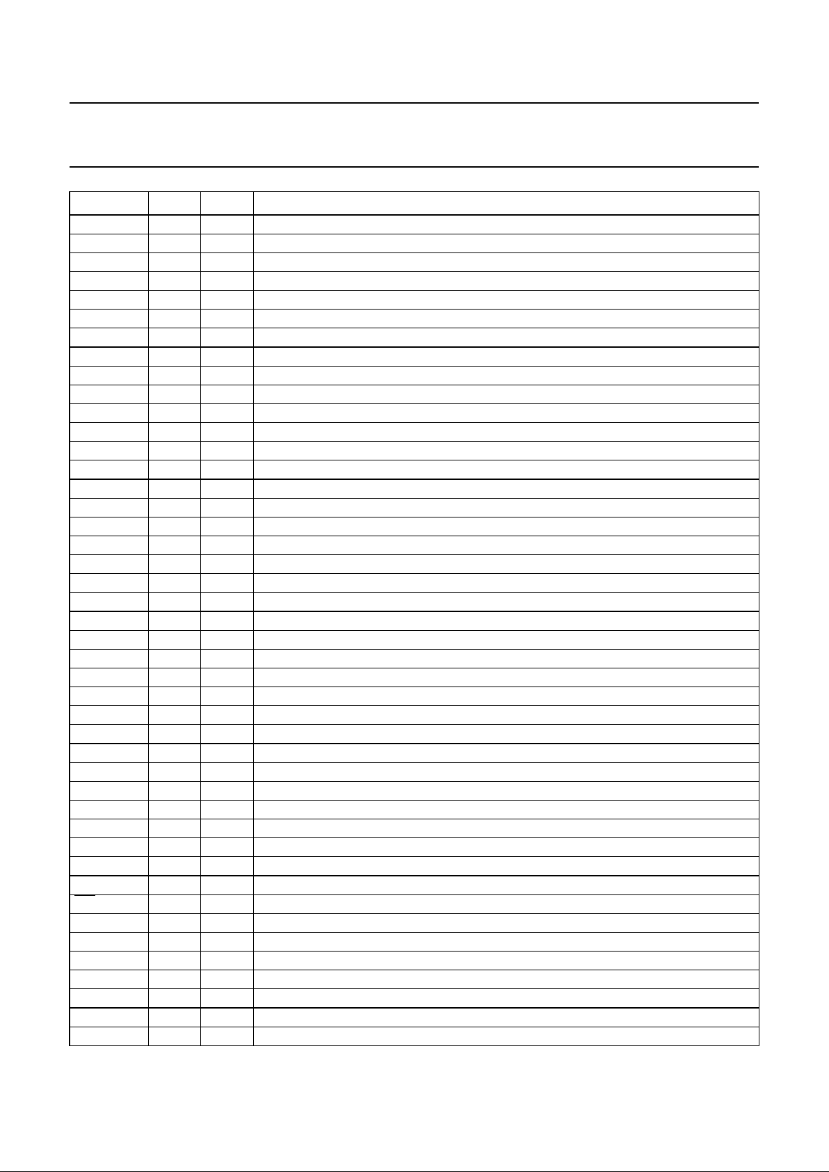
1998 Feb 13 5
Philips Semiconductors Product specification
Satellite Demodulator and Decoder (SDD) TDA8043
V
SSD3
18 − digital ground 3
V
DDD2
19 − digital supply voltage 2
PRESET 20 I set device into default mode
P3 21 I/O quasi-bidirectional I/O port (bit 3)
P2 22 I/O quasi-bidirectional I/O port (bit 2)
P1 23 I/O quasi-bidirectional I/O port (bit 1)
P0 24 I/O quasi-bidirectional I/O port (bit 0)
V
DDD3
25 − digital supply voltage 3
n.c. 26 − not connected
n.c. 27 − not connected
PDOCLK 28 O output clock for transport stream bytes
PDO0 29 O parallel data output (bit 0)
PDO1 30 O parallel data output (bit 1)
PDO2 31 O parallel data output (bit 2)
V
SSD4
32 − digital ground 4
PDO3 33 O parallel data output (bit 3)
PDO4 34 O parallel data output (bit 4)
PDO5 35 O parallel data output (bit 5)
n.c. 36 − not connected
n.c. 37 − not connected
PDO6 38 O parallel data output (bit 6)
n.c. 39 − not connected
V
DDD4
40 − digital supply voltage 4
V
DDD5
41 − digital supply voltage 5
V
SSD5
42 − digital ground 5
V
DDD6
43 − digital supply voltage 6
V
DDD7
44 − digital supply voltage 7
PDO7 45 O parallel data output (bit 7)
n.c. 46 − not connected
n.c. 47 − not connected
PDOERR 48 O transport error indicator
PDOVAL 49 O data valid indicator
PDOSYNC 50 O transport packet synchronization signal
V
SSD6
51 − digital ground 6
SCL 52 I serial clock of I
2
C-bus; note 1
SDA 53 I/O serial data of I
2
C-bus; note 1
INT 54 O interrupt output (active LOW); note 1
A0 55 I I
2
C hardware address; note 1
RSLOCK 56 O Reed-Solomon lock indicator
VLOCK 57 O Viterbi lock indicator
DLOCK 58 O demodulator lock indicator
V
DDD8
59 − digital supply voltage 8
V
DDD9
60 − digital supply voltage 9
TEST 61 I test pin (normally connected to ground); note 1
SYMBOL PIN I/O DESCRIPTION
 Loading...