

Philips TDA8042M-C1 Datasheet

DATA SH EET
Product specification
File under Integrated Circuits, IC02
1997 Apr 11
INTEGRATED CIRCUITS
TDA8042M
Quadrature demodulator

1997 Apr 11 2
Philips Semiconductors Product specification
Quadrature demodulator TDA8042M
FEATURES
• 5 V supply voltage
• Internal voltage reference
• 350 to 650 MHz input frequency range
• On-chip 0° and 90° phase shifter
• Symbol rate up to 45 Msymbols/s
• High input sensitivity
• Built-in voltage stabilizer
• AGC amplifier with 21 dB control range
• AGC detector.
APPLICATION
• Binary Phase-Shift Keying (BPSK) and Quadrature
Phase-Shift Keying (QPSK) demodulation.
GENERAL DESCRIPTION
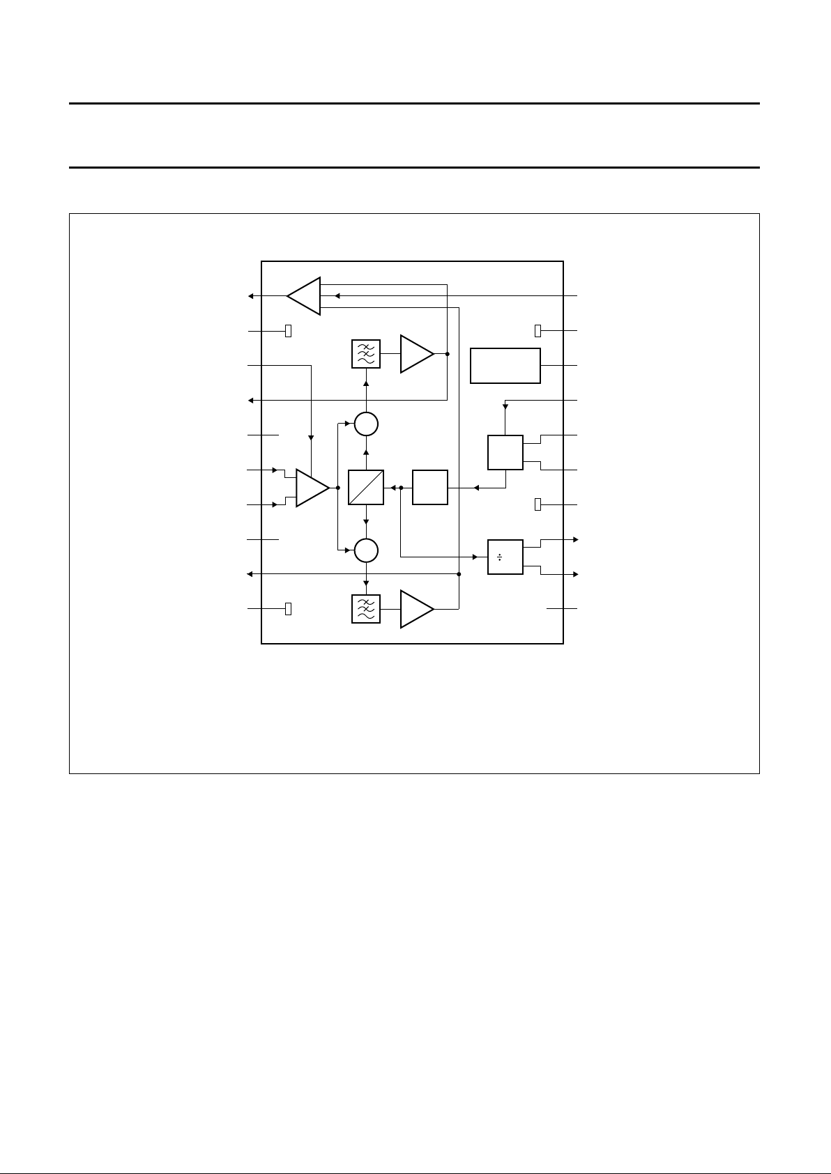
The TDA8042M is a monolitic bipolar IC dedicated for
BPSK and QPSK demodulation. It is designed to be used
together with the TDA8043 as part of a complete
BPSK/QPSK satellite demodulator and decoder.
The bandwidth of the TDA8042M allows symbol rates up
to 45 Msymbols/s. It includes two matched mixers, an IF
gain controlled amplifier, a symmetrical oscillator, a 0°/90°
phase shifter, two low-pass filters and two matched
baseband amplifiers.
The high input sensitivity makes interfacing with various
sources easy. The input sensitivity can be adjusted by
means of an internal AGC amplifier.
The oscillator operates at half the IF frequency. The local
oscillator signal driving the mixers is made by doubling the
oscillator frequency by an internal frequency multiplier.
The oscillator frequency can be set by the appropriate
external LC tank circuit. The internal wideband phase
shifter provides two oscillator signals which are
90 degrees out of phase to drive the mixers.
An AGC detector at the I and Q outputs makes it possible
to keep the I and Q signals at a constant level to drive the
analog-to-digital converters of the TDA8043.
QUICK REFERENCE DATA
ORDERING INFORMATION
SYMBOL PARAMETER CONDITIONS MIN. TYP. MAX. UNIT
V
CC
supply voltage 4.75 5.0 5.25 V
I
CC
supply current VCC= 5.0 V 54 67.5 81 mA
V
i(RF)
operating input level − 57 − dBµV
f
i(RF)
RF input signal frequency 350 − 650 MHz
V
olQ(p-p)
I and Q output voltage (peak-to-peak value) − 0.8 − V
∆E
Φ(I-Q)
phase matching error between I and Q channels − 0.7 2 deg
∆E
G(I-Q)
gain matching error between I and Q channels − 0.15 0.8 dB
∆G
tilt
gain tilt error between I and Q channels − 0.3 0.5 dB
TYPE
NUMBER
PACKAGE
NAME DESCRIPTION VERSION
TDA8042M SSOP20 plastic shrink small outline package; 20 leads; body width 4.4 mm SOT266-1
1997 Apr 11 3
Philips Semiconductors Product specification
Quadrature demodulator TDA8042M
BLOCK DIAGRAM
Fig.1 Block diagram.
handbook, full pagewidth
MBH968
DET
I
VOLTAGE
REFERENCE
×
1
2
10
3
5
8
9
6
7
4
Q
×
90°
0°
× 2
VCO
32
20
19
11
14
18
16
15
13
12
17
IDET
VTH
GND1
GND1
VAGC
V
CC1
IOUT
OSCDIS
GND2
OSCA
IFA
OSCB
IFB
GND1
V
CC2
FDIV(A)
QOUT FDIV(B)
GND1
V
CC1
TDA8042M
1997 Apr 11 4
Philips Semiconductors Product specification
Quadrature demodulator TDA8042M
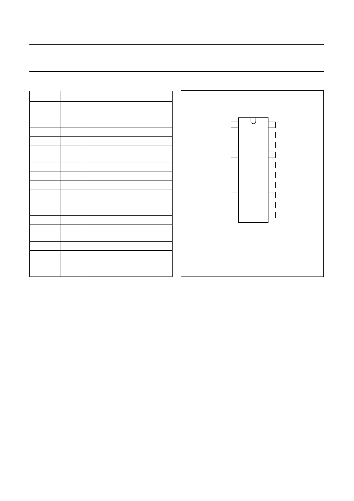
PINNING
SYMBOL PIN DESCRIPTION
IDET 1 AGC detector output signal
GND1 2 ground
VAGC 3 gain control input voltage
IOUT 4 I channel amplifier output
GND2 5 ground
IFA 6 IF input A
IFB 7 IF input B
V
CC2
8 supply voltage 2
QOUT 9 Q channel amplifier output
GND1 10 ground
V
CC1
11 supply voltage 1
FDIV(B) 12 prescaler output B
FDIV(A) 13 prescaler output A
GND1 14 ground
OSCB 15 oscillator tank circuit B
OSCA 16 oscillator tank circuit A
OSCDIS 17 oscillator disable input
V
CC1
18 supply voltage 1
GND1 19 ground
VTH 20 AGC threshold voltage input
Fig.2 Pin configuration.
handbook, halfpage
TDA8042M
MBH967
1
2
3
4
5
6
7
8
9
10
20
19
18
17
16
15
14
13
12
11
IDET VTH
GND1 GND1
VAGC V
CC1
IOUT OSCDIS
GND2 OSCA
IFA OSCB
IFB GND1
V
CC2
FDIV(A)
QOUT FDIV(B)
GND1 V
CC1

1997 Apr 11 5
Philips Semiconductors Product specification
Quadrature demodulator TDA8042M
LIMITING VALUES
In accordance with the Absolute Maximum Rating System (IEC 134).
Note
1. The operating ambient temperature can be extended up to +85 °C providing the supply voltage remains lower or
equal to 5.2 V in order to maintain the junction temperature below 150 °C.
QUALITY SPECIFICATION
All pins withstand the ESD test in accordance with
“UZW-BO/FQ-A302 (human body model)”
and with
“UZW-BO/FQ-B302 (machine model)”
. These numbers can be found in the
“Quality reference Handbook”
. The handbook
can be ordered using the code 9397 750 00192.
THERMAL CHARACTERISTICS
SYMBOL PARAMETER MIN. MAX. UNIT
V
CC
supply voltage −0.3 +6.0 V
V
i
input voltage on all pins −0.3 V
CC
V
P
tot
total power dissipation − 470 mW
T
stg
IC storage temperature −55 +150 °C
T
j
junction temperature − +150 °C
T
amb
operating ambient temperature 0 +70
(1)
°C
SYMBOL PARAMETER VALUE UNIT
R
th j-a
thermal resistance from junction to ambient in free air 120 K/W
 Loading...