

Philips tda6404, tda 6405 DATASHEETS
INTEGRATED CIRCUITS
DATA SH EET
TDA6404; TDA6405; TDA6405A
5 V mixer/oscillator-PLL
synthesizers for hyperband tuners
Product specification
Supersedes data of 1998 Jan 19
File under Integrated Circuits, IC02
1999 Jan 13

Philips Semiconductors Product specification
5 V mixer/oscillator-PLL synthesizers
for hyperband tuners
FEATURES
• Single chip 5 V mixer/oscillator-PLL synthesizer for
hyperband tuners
• I2C-bus protocol
• 3 PNP band switch buffers (25 mA)
• 33 V tuning voltage output
• In-lock detector
• 5-level Analog-to-Digital Converter (ADC)
• 15-bit programmable divider
• Programmable reference divider ratio
(512, 640 or 1024)
• Programmable charge pump current
• Balanced mixer with a common emitter input for VHF
(single input)
• Balanced mixer with a common base input for UHF
(double input)
• 4-pin common emitter oscillator for VHF
• 4-pin common emitter oscillator for UHF
• IF amplifier with a low output impedance to drive a SAW
filter directly (≈2kΩ load)
• Low power, low radiation, small size
APPLICATIONS
• Hyperband tuners for Europe using a 2-band
mixer/oscillator in a switched concept.
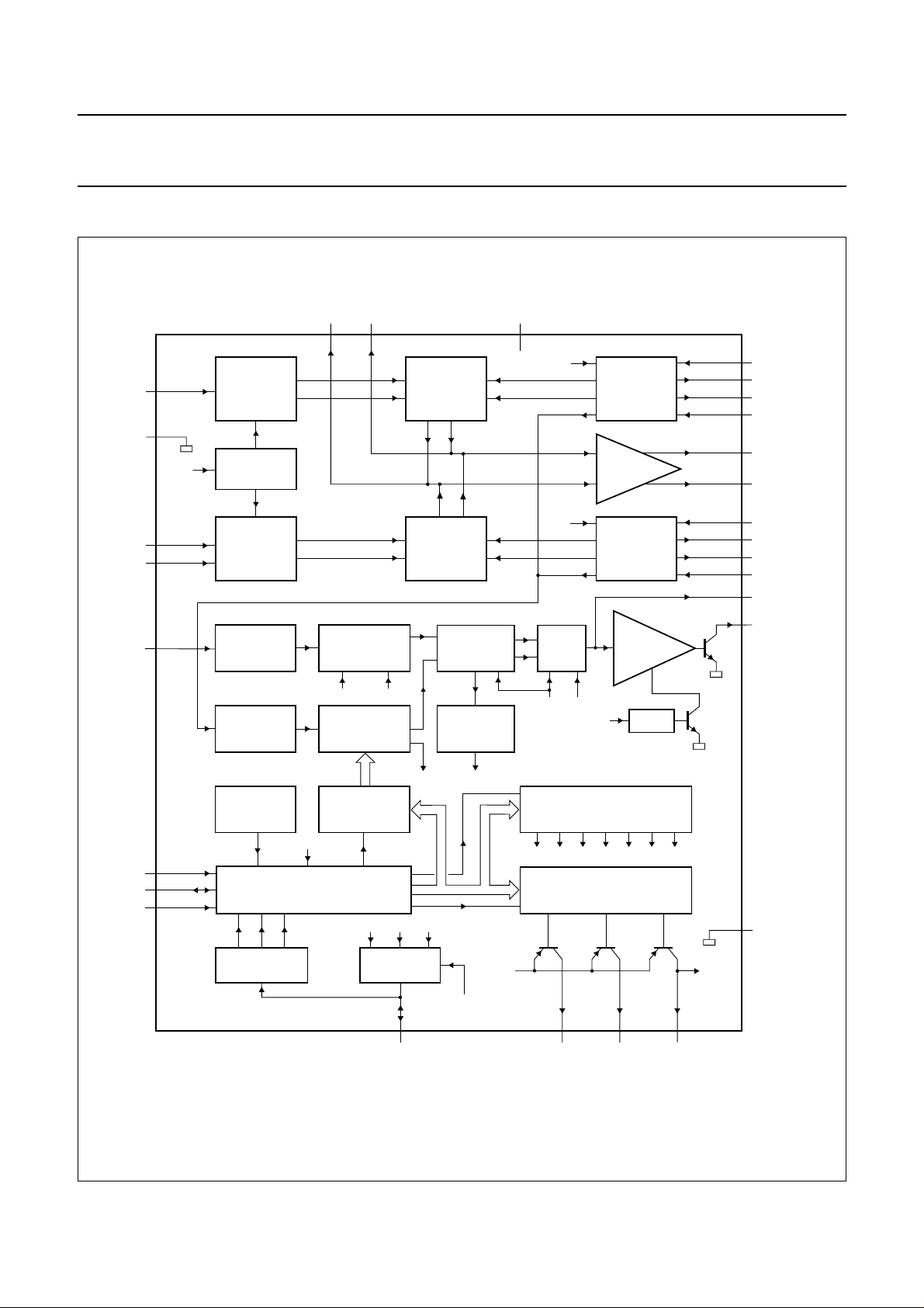
GENERAL DESCRIPTION
The TDA6404, TDA6405 and TDA6405A are
programmable 2-band mixer/oscillator-PLL synthesizers
intended for VHF/UHF and hyperband tuners (see Fig.1).
The devices include two double balanced mixers and two
oscillators for the VHF and UHF band, an IF amplifier and
a PLL synthesizer. With proper oscillator application and
by using a switchable inductor to split the VHF band into
two sub-bands (the full VHF/UHF and hyperband) the TV
bands can be covered.
TDA6404; TDA6405;
TDA6405A
The PLL synthesizer consists of a divide-by-eight
prescaler, a 15-bit programmable divider, a 4 MHz crystal
oscillator and its programmable reference divider and a
phase comparator combined with a charge pump which
drives the tuning amplifier, including 33 V output.
Depending on the reference divider ratio (512, 640
or 1024), the phase comparator operates at 7.8125 kHz,
6.25 kHz or 3.90625 kHz.
2
The devices are controlled according to the I
format. The in-lock detector bit FL is set to logic 1 when the
loop is locked and is read on the SDA line (status byte)
during a read operation. The ADC input is available for
digital Automatic Frequency Control (AFC). The ADC code
is read during a read operation on the I2C-bus
(see Table 9). In test mode, pin ADC is used as a test
output for f
When the charge pump current switch mode is activated
and the loop is phase-locked the charge pump current
value is automatically switched to LOW. This is to improve
carrier-to-noise ratio. The status of this feature can be read
in the ACPS flag during a read operation on the I2C-bus
(see Table 7).
Five serial bytes (including address byte) are required for
the I2C-bus format to address the devices, select the VCO
frequency, program the three PNP ports, set the charge
pump current and to set the reference divider ratio.
The devices have four independent I2C-bus addresses
which can be selected by applying a specific voltage on the
AS input (see Table 4).
REF
and1⁄2f
DIV
.
C-bus
Two pins are available between the mixer output and the
IF amplifier input to enable IF filtering for improved signal
handling. Three PNP ports are provided for band
switching. Band selection is made according to the band
switch bits VHFL, VHFH and UHF.
1999 Jan 13 2
Philips Semiconductors Product specification
5 V mixer/oscillator-PLL synthesizers for
hyperband tuners
TDA6404; TDA6405;
TDA6405A
QUICK REFERENCE DATA
SYMBOL PARAMETER CONDITIONS MIN. TYP. MAX. UNIT
V
CC
I
CC
f
XTAL
I
o(PNP)
T
stg
T
amb
f
(i)RF
supply voltage operating 4.5 5 5.5 V
supply current all PNP ports are ‘OFF’ − 78 − mA
crystal oscillator frequency R
= 25 to 150 Ω 3.2 4.0 4.48 MHz
XTAL
PNP port output current −−25 mA
IC storage temperature −40 − +150 °C
operating ambient temperature −20 − +85 °C
RF input frequency VHF band 45.25 − 399.25 MHz
UHF band 407.25 − 855.25 MHz
G
V
voltage gain VHF band − 27 − dB
UHF band − 38 − dB
F noise figure VHF band − 8 − dB
UHF band − 8.5 − dB
V
o
output voltage causing 1% cross
modulation in channel
VHF band − 119 − dBµV
UHF band − 118 − dBµV
ORDERING INFORMATION
TYPE
NUMBER
NAME DESCRIPTION VERSION
TDA6404TS;
TDA6405TS;
SSOP28 plastic shrink small outline package; 28 leads; body width 5.3 mm SOT341-1
TDA6405ATS
PACKAGE
1999 Jan 13 3
Philips Semiconductors Product specification
5 V mixer/oscillator-PLL synthesizers for
hyperband tuners
BLOCK DIAGRAM
IFFIL1
handbook, full pagewidth
XTAL
3 (26)
4 (25)
1 (28)
2 (27)
16 (13)
VHFIN
RFGND
UHFIN1
UHFIN2
BS
RF INPUT
VHF
BSVHF
ELECTRONIC
BAND SWITCH
BSUHF
RF INPUT
UHF
XTAL
OSCILLATOR
4 MHz
IFFIL2
5 (24) 17 (12)
6 (23)
VHF
MIXER
UHF
MIXER
f
REFERENCE
DIVIDER
512, 640, 1024
REF
DIGITAL
PHASE
COMPARATOR
TDA6404; TDA6405;
TDA6405A
V
CC
BSVHF
BSUHF
CHARGE
PUMP
VHF
OSCILLATOR
IF
AMPLIFIER
UHF
OSCILLATOR
TUNING
AMPLIFIER
(4) 25
(3) 26
(2) 27
(1) 28
(11) 18
(10) 19
(5) 24
(6) 23
(7) 22
(8) 21
(15) 14
(14) 15
VHFOSCIB1
VHFOSCOC1
VHFOSCOC2
VHFOSCIB2
IFOUT1
IFOUT2
UHFOSCIB2
UHFOSCOC2
UHFOSCOC1
UHFOSCIB1
CP
VT
f
DIV
1/2f
DIV
f
1/2f
REF
DIV
GATE
13 (16) 7 (22) 8 (21) 9 (20)
ADC
SCL
SDA
AS
12 (17)
11 (18)
10 (19)
PRESCALER
DIVIDE BY 8
POWER-ON
RESET
SCL
SDA
AS
5-LEVEL A/D
CONVERTER
RSA
15-BIT
PROGRAMMABLE
DIVIDER
15-BIT
FREQUENCY
REGISTER
FL
I2C-BUS
TRANSCEIVER
RSB
FL
The pin numbers in parenthesis represent the TDA6405 and TDA6405A.
IN-LOCK
DETECTOR
FL
T2, T1, T0
T2, T1, T0
CHP
TDA6404
TDA6405
TDA6405A
7-BIT CONTROL
T2 T1 T0 RSA RSB OSCHP
3-BIT BAND SWITCH
VHFL VHFH UHF
V
CC
PVHFL
OS
REGISTER
REGISTER
PVHFH
LOGIC
PUHF
BS
(9) 20
MGK813
GND
Fig.1 Block diagram.
1999 Jan 13 4
Philips Semiconductors Product specification
5 V mixer/oscillator-PLL synthesizers for
TDA6404; TDA6405;
hyperband tuners
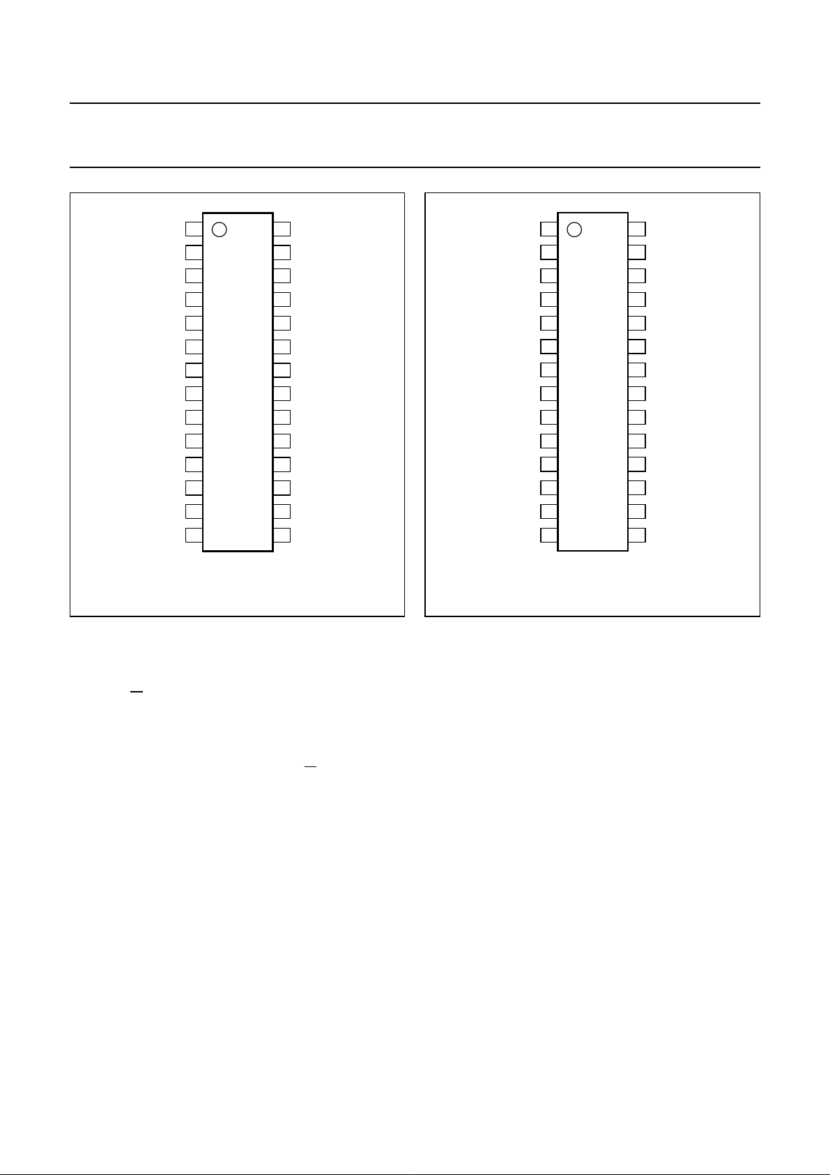
PINNING
PIN
SYMBOL
UHFIN1 1 28 UHF input 1
UHFIN2 2 27 UHF input 2
VHFIN 3 26 VHF input
RFGND 4 25 RF ground
IFFIL1 5 24 IF filter output 1
IFFIL2 6 23 IF filter output 2
PVHFL 7 22 PNP port output for VHF low band
PVHFH 8 21 PNP port output for VHF high band
PUHF 9 20 PNP port output for UHF band
AS 10 19 address selection input
SDA 11 18 serial data input/output (I
SCL 12 17 serial clock input (I
ADC 13 16 Analog-to-Digital Converter input/output
CP 14 15 charge pump output
VT 15 14 tuning output
XTAL 16 13 crystal oscillator input
V
CC
IFOUT1 18 11 IF amplifier output 1
IFOUT2 19 10 IF amplifier output 2
GND 20 9 ground
UHFOSCIB1 21 8 UHF oscillator base input 1
UHFOSCOC1 22 7 UHF oscillator collector output 1
UHFOSCOC2 23 6 UHF oscillator collector output 2
UHFOSCIB2 24 5 UHF oscillator base input 2
VHFOSCIB1 25 4 VHF oscillator base input 1
VHFOSCOC1 26 3 VHF oscillator collector output 1
VHFOSCOC2 27 2 VHF oscillator collector output 2
VHFOSCIB2 28 1 VHF oscillator base input 2
TDA6404
17 12 supply voltage
TDA6405;
TDA6405A
DESCRIPTION
2
2
C-bus)
C-bus)
TDA6405A
1999 Jan 13 5
Philips Semiconductors Product specification
5 V mixer/oscillator-PLL synthesizers for
hyperband tuners
handbook, halfpage
UHFIN1
UHFIN2
VHFIN
RFGND
IFFIL1
IFFIL2
PVHFL
PVHFH
PUHF
AS
SDA
SCL
ADC
CP
1
2
3
4
5
6
7
8
9
10
11
12
13
TDA6404
MGK830
VHFOSCIB2
28
VHFOSCOC2
27
VHFOSCOC1
26
VHFOSCIB1
25
UHFOSCIB2
24
23
UHFOSCOC2
UHFOSCOC1
22
21
UHFOSCIB1
GND
20
IFOUT2
19
IFOUT1
18
V
17
CC
XTAL
16
1514
VT
handbook, halfpage
VHFOSCIB2
VHFOSCOC2
VHFOSCOC1
VHFOSCIB1
UHFOSCIB2
UHFOSCOC2
UHFOSCOC1
UHFOSCIB1
GND
IFOUT2
IFOUT1
V
CC
XTAL
VT
TDA6404; TDA6405;
TDA6405A
1
2
3
4
5
6
7
TDA6405
TDA6405A
8
9
10
11
12
13
MGK831
28
27
26
25
24
23
22
21
20
19
18
17
16
1514
UHFIN1
UHFIN2
VHFIN
RFGND
IFFIL1
IFFIL2
PVHFL
PVHFH
PUHF
AS
SDA
SCL
ADC
CP
Fig.2 Pin configuration for TDA6404.
FUNCTIONAL DESCRIPTION
The devices are controlled via the I2C-bus.
For programming, there is one module address (7 bits)
and the R/W bit for selecting the read or write mode.
Write mode
Data bytes can be sent to the devices after the address
transmission (first byte) by setting the R/
W bit to logic 0.
Four data bytes are needed to fully program the devices.
The I2C-bus transceiver has an auto-increment facility
which permits the programming of the devices within one
single transmission (address + 4 data bytes).
The devices can also be partially programmed, providing
that the first data byte following the address is divider
byte 1 (DB1) or control byte (CB). The bits in the data
bytes are defined in Tables 1 and 2.
Fig.3 Pin configuration for TDA6405(A)
The first bit of the data byte transmitted indicates whether
frequency data (first bit = 0) or control and band switch
data (first bit = 1) will follow. Until an I
2
C-bus STOP
condition is sent by the controller, additional data bytes
can be entered without the need to re-address the devices.
The frequency register is loaded after the 8th clock pulse
of the second divider byte (DB2). The control register is
loaded after the 8th clock pulse of the CB. The band switch
register is loaded after the 8th clock pulse of the band
switch byte (BB).
1999 Jan 13 6
Philips Semiconductors Product specification
5 V mixer/oscillator-PLL synthesizers for
hyperband tuners
Table 1 I2C-bus mode, write data format for the TDA6404 and TDA6405
NAME BYTE
Address byte ADB 11000MA1MA0R/
Divider byte 1 DB1 0 N14 N13 N12 N11 N10 N9 N8 A
Divider byte 2 DB2 N7 N6 N5 N4 N3 N2 N1 N0 A
Control byte CB 1 CHP T2 T1 T0 RSA RSB OS A
Band-switch byte BB XXXXXUHFVHFH VHFL A
2
Table 2 I
Address byte ADB 11000MA1MA0R/
Divider byte 1 DB1 0 N14 N13 N12 N11 N10 N9 N8 A
Divider byte 2 DB2 N7 N6 N5 N4 N3 N2 N1 N0 A
Control byte CB 1 CHP T2 T1 T0 RSA RSB OS A
Band-switch byte BB XXXXUHFXVHFH VHFL A
C-bus mode, write data format for the TDA6405A
NAME BYTE
MSB LSB
MSB LSB
BITS
BITS
TDA6404; TDA6405;
TDA6405A
W=0 A
W=0 A
ACK
ACK
2
C-bus address selection
I
The module address contains programmable address bits (MA1 and MA0) which offer the possibility of having several
synthesizers (up to 4) in one system by applying a specific voltage on the AS input. The relationship between MA1 and
MA0 and the input voltage applied to the AS input is given in Table 4.
Table 3 Description of symbols used in Tables 1 and 2
SYMBOL DESCRIPTION
A acknowledge
MA1 and MA0 programmable address bits (see Table 4)
N14 to N0 programmable divider bits; N = N14 × 2
CHP charge pump current bit:
CHP = 0; ICP=60µA
CHP = 1; I
T2, T1 and T0 test bits (see Table 5)
RSA and RSB reference divider ratio select bits (see Table 6)
OS tuning amplifier control bit:
OS = 0; normal operation; tuning voltage is ‘ON’
OS = 1; tuning voltage is ‘OFF’ (high-impedance)
UHF, VHFH and VHFL PNP ports control bits:
bit = 0; buffer n is ‘OFF’ (default)
bit = 1; buffer n is ‘ON’
X don’t care bit: may be a logic 0 or a logic 1
= 280 µA (default)
CP
14
+ N13 × 213+ ... + N1 × 21+N0
1999 Jan 13 7
Philips Semiconductors Product specification
5 V mixer/oscillator-PLL synthesizers for
hyperband tuners
Table 4 Address selection I2C-bus
MA1 MA0 VOLTAGE APPLIED ON AS INPUT
0 0 0 to 0.1V
0 1 open or 0.2VCCto 0.3V
1 0 0.4VCCto 0.6V
1 1 0.9VCCto 1.0V
Table 5 Test mode
T2 T1 T0 TEST MODES
0 0 0 automatic charge pump off
0 0 1 automatic charge pump on; note 1
0 1 X charge pump is ‘OFF’
1 1 0 charge pump is sinking current
1 1 1 charge pump is sourcing current
100f
101
CC
REF
1
⁄
2
CC
CC
CC
is available on pin ADC; note 2
f
is available on pin ADC; note 2
DIV
TDA6404; TDA6405;
TDA6405A
Notes
1. This is the default mode at Power-on reset.
2. The ADC input cannot be used when these test modes are active.
Table 6 Reference divider ratio select bits
RSA RSB REFERENCE DIVIDER RATIO FREQUENCY STEP (kHz)
X 0 640 6.25
0 1 1024 3.90625
1 1 512 7.8125
Read mode
Data can be read from the devices by setting the R/W bit
to logic 1 (see Tables 7 and 8). After the slave address
has been recognized, the devices generate an
acknowledge pulse and the first data byte (status byte) is
transferred on the SDA line (MSB first). Data is valid on the
SDA line during a HIGH-level of the SCL clock signal.
A second data byte can be read from the devices if the
The ACPS flag is LOW when the automatic charge pump
switch mode is ‘ON’ and the loop is locked. In other
conditions, ACPS = 1. When ACPS = 0, the charge pump
current is forced to the LOW value.
A built-in ADC is available on ADC pin. This converter can
be used to apply AFC information to the controller from the
IF section of the television. The relationship between the
bits A2, A1 and A0 is given in Table 9.
processor generates an acknowledge on the SDA line
(master acknowledge). End of transmission will occur if no
master acknowledge occurs. The devices will then release
the data line to allow the processor to generate a STOP
condition. The POR flag is set to logic 1 at power-on.
The flag is reset when an end-of-data is detected by the
devices (end of a read sequence). Control of the loop is
made possible with the in-lock flag FL which indicates
when the loop is locked (FL = 1).
1999 Jan 13 8
Philips Semiconductors Product specification
5 V mixer/oscillator-PLL synthesizers for
hyperband tuners
TDA6404; TDA6405;
TDA6405A
Table 7 Read data format
BITS
NAME BYTE
Address byte ADB 1 1000MA1MA0R/
MSB
(1)
LSB
W=1 A
Status byte SB POR FL ACPS 1 1 A2 A1 A0 −
Note
1. MSB is transmitted first.
Table 8 Description of symbols used in Table 7
SYMBOL DESCRIPTION
A acknowledge
POR Power-on reset flag (POR = 1 at power-on)
FL in-lock flag (FL = 1 when the loop is locked)
ACPS automatic charge pump switch flag:
ACPS = 0; active
ACPS = 1; not active
A2, A1 and A0 digital outputs of the 5-level ADC (see Table 9)
ACK
Table 9 Analog-to-digital converter levels; note 1
A2 A1 A0 VOLTAGE APPLIED ON ADC INPUT
1 0 0 0.60V
0 1 1 0.45VCCto 0.60V
0 1 0 0.30VCCto 0.45V
0 0 1 0.15VCCto 0.30V
0 0 0 0 to 0.15V
Note
1. Accuracy is ±0.03V
CC
.
Power-on reset
The power-on detection threshold voltage V
POR
is set to
VCC= 2 V at room temperature. Below this threshold, the
device is reset to the power-on state.
At power-on state, the charge pump current is set to
280 µA, the tuning voltage output is disabled, the test
bits T2, T1 and T0 are set to logic 001 (automatic charge
pump switch ‘ON’) and RSB is set to logic 1.
to 1.00V
CC
CC
CC
CC
CC
CC
PUHF is ‘OFF’, which means that the UHF oscillator and
the UHF mixer are switched off. Consequently, the VHF
oscillator and the VHF mixer are switched on. PVHFL and
PVHFH are ‘OFF’, which means that the VHF tank circuit
is working in the VHF I sub-band. The tuning amplifier is
switched off until the first transmission. In that case, the
tank circuit in VHF I is supplied with the maximum tuning
voltage. The oscillator is therefore working at the end of
the VHF I sub-band.
1999 Jan 13 9
Philips Semiconductors Product specification
5 V mixer/oscillator-PLL synthesizers for
hyperband tuners
TDA6404; TDA6405;
TDA6405A
Table 10 Default bits at Power-on reset
BITS
NAME BYTE
MSB LSB
Address byte ADB 11000MA1MA0X
Divider byte 1 DB1 0 XXXXXXX
Divider byte 2 DB2 XXXXXXXX
Control byte CB 11001X10
Band-switch byte BB XXXX0000
LIMITING VALUES
In accordance with the Absolute Maximum Rating System (IEC 134) (note 1).
SYMBOL PARAMETER MIN. MAX. UNIT
V
CC
V
O(n)
I
O(n)
V
O(CP
V
O(VT)
V
I/O(ADC)
V
I(SCL)
V
I/O(SDA)
I
O(SDA)
V
I(AS)
V
I(XTAL)
I
O(n)
supply voltage −0.3 +6 V
output voltage on pins PVHFL, PVHFH and PUHF −0.3 +6 V
output current on pins PVHFL, PVHFH and PUHF −1 +30 mA
) charge pump output voltage −0.3 +6 V
tuning output voltage −0.3 +35 V
ADC input/output voltage −0.3 +6 V
serial clock input voltage −0.3 +6 V
serial data input/output voltage −0.3 +6 V
data output current −1 +10 mA
address selection input voltage −0.3 +6 V
crystal oscillator input voltage −0.3 +6 V
output current of each pin to ground:
for TDA6404, pins 1 to 6 and 17 to 28 −−10 mA
for TDA6405 and TDA6405A, pins 1 to 12 and 23 to 28 −−10 mA
t
sc(max)
T
stg
T
amb
T
j
maximum short-circuit time (all pins to VCC and all pins to GND, RFGND) − 10 s
IC storage temperature −40 +150 °C
operating ambient temperature −20 +85 °C
junction temperature − 150 °C
Note
1. Maximum ratings can not be exceeded, not even momentarily without causing irreversible IC damage.
Maximum ratings can not be accumulated.
THERMAL CHARACTERISTICS
SYMBOL PARAMETER CONDITIONS TYPICAL UNIT
R
th(j-a)
thermal resistance from junction to ambient in free air 85 K/W
1999 Jan 13 10
 Loading...