


INTEGRATED CIRCUITS
DATA SH EET
TDA4882
Advanced monitor video controller
for OSD
Product specification
Supersedes data of December 1994
File under Integrated Circuits, IC02
1997 Sep 04

Philips Semiconductors Product specification
Advanced monitor video controller for OSD TDA4882
CONTENTS
1 FEATURES
2 GENERAL DESCRIPTION
3 QUICK REFERENCE DATA
4 ORDERING INFORMATION
5 BLOCK DIAGRAM
6 PINNING
7 FUNCTIONAL DESCRIPTION
7.1 General
7.2 Brightness control
7.3 Contrast control
7.4 Output stages
7.5 Input clamping
7.6 Vertical blanking
7.7 Horizontal blanking
7.8 Cut-off and black-level stabilization
7.9 On Screen Display
7.10 Test mode
8 LIMITING VALUES
9 THERMAL CHARACTERISTICS
10 CHARACTERISTICS
11 APPLICATION AND TEST INFORMATION
11.1 Recommendations for building the application
board
12 INTERNAL PIN CONFIGURATION
13 PACKAGE OUTLINE
14 SOLDERING
14.1 Introduction
14.2 Soldering by dipping or by wave
14.3 Repairing soldered joints
15 DEFINITIONS
16 LIFE SUPPORT APPLICATIONS
1997 Sep 04 2

Philips Semiconductors Product specification
Advanced monitor video controller for OSD TDA4882
1 FEATURES
• 85 MHz video controller
• Fully DC controllable
• 3 separate video channels
• Input black-level clamping
2 GENERAL DESCRIPTION
The TDA4882 is an RGB pre-amplifier for colour monitor
systems with SVGA performance, intended for DC or AC
coupling of the colour signals to the cathodes of the CRT.
With special advantages the circuit can be used in
conjunction with the TDA485x monitor deflection IC family.
• White level adjustment for 2 channels only
• Brightness control with correct grey scale tracking
• Contrast control for all 3 channels simultaneously
• Cathode feedback to internal reference for cut-off
control, which allows unstabilized video supply voltage
• Current outputs for RGB signal currents
• RGB voltage outputs to external peaking circuits
• Blanking and switch-off input for screen protection
• Sync on green operation possible
• On Screen Display (OSD) facility.
3 QUICK REFERENCE DATA
SYMBOL PARAMETER CONDITIONS MIN. TYP. MAX. UNIT
V
P
I
P
V
i(b-w)
V
o(b-w)
positive supply voltage 7.2 8.0 8.8 V
supply current 36 48 60 mA
input voltage, black-to-white − 0.7 1.0 V
output voltage, black-to-white nominal contrast;
− 0.79 − V
channels 1 and 3 gain
control pins open-circuit
I
o(b-w)
I
OM
output current, black-to-white − 50 − mA
peak output current −−100 mA
B bandwidth −3dB 70 85 − MHz
G
nom
nominal voltage gain nominal contrast;
− 1 − dB
channels 1 and 3 gain
control pins open-circuit
∆G gain control difference for 2 channels relative to G
CR
contrast
C
OSD(min)
∆V
bl
contrast control V
minimum contrast for OSD V
brightness control related to nominal
=1to6V −22 − +3.4 dB
i(CC)
= 0.7 V −−40 − dB
i(CC)
nom
−5 − +2.6 dB
−11 − +34 %
output signal amplitude
T
amb
operating ambient temperature −20 − +70 °C
4 ORDERING INFORMATION
TYPE
NUMBER
NAME DESCRIPTION VERSION
PACKAGE
TDA4882 DIP20 plastic dual in-line package; 20 leads (300 mil) SOT146-1
1997 Sep 04 3
Philips Semiconductors Product specification
Advanced monitor video controller for OSD TDA4882
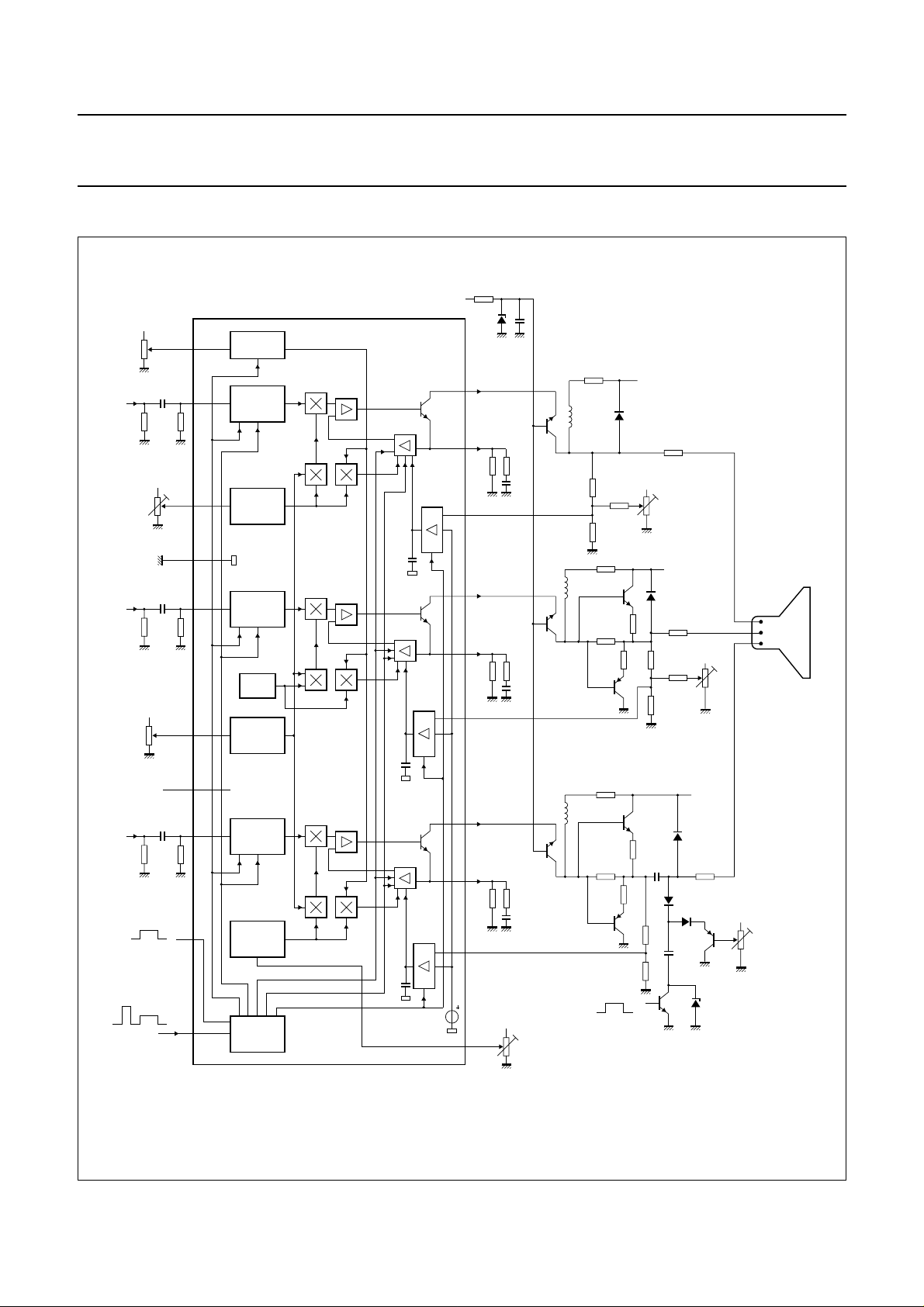
5 BLOCK DIAGRAM
handbook, full pagewidth
V
P
10 kΩ
brightness
control
signal
22 nF
input
75 Ω
10 MΩ
V
P
10 kΩ
gain
control
signal
22 nF
input
75 Ω
10 MΩ
V
P
10 kΩ
contrast
control
VP = 8 V
VOLTAGE
1
CONVERTER
2
3
4
5
6
CLAMP
CLIPPING
VOLTAGE
CONVERTER
CLAMP
CLIPPING
REF
GAIN
VOLTAGE
CONVERTER
CHANNEL 1
CHANNEL 2
TDA4882
20
19
18
17
16
15
6.2 V
current
output
voltage
output
33 Ω 33 Ω
feedback
current
output
voltage
output
33 Ω 33 Ω
feedback
BFQ235
BFQ235
1.5 kΩ
68 kΩ
6.8 kΩ
1.5 kΩ
BFQ236
1 kΩ
BFQ256
10 Ω
15 kΩ
10 Ω
BAV21
V
= 90 V
CRT
220 Ω
8 V
10 kΩ
cut-off
control
V
= 90 V
CRT
BAV21
220 Ω
68 kΩ
15 kΩ
6.8 kΩ
40 MHz
8 V
10 kΩ
cut-off
control
25 MHz
CRT
60 MHz
P
22 nF
10 MΩ
7
8
9
10
input
clamping
blanking
+
CLAMP
CLIPPING
VOLTAGE
CONVERTER
PULSE
DECODER
CHANNEL 3
test mode
ultra black
output clamping
5.8 V
V
signal
input
75 Ω
horizontal blanking
switch off
clamping pulse
vertical blanking
test mode
Fig.1 Block diagram and basic application circuits for DC and AC coupling.
1997 Sep 04 4
14
13
12
11
current
output
voltage
output
18 Ω
feedback
10 kΩ
V
18 Ω
P
gain
control
BFQ235
860 Ω
10 Ω
1 kΩ
10 Ω
BFQ256
10 kΩ
horizontal blanking
BFQ236
47 nF
V
= 65 V
CRT
BAV21
100 Ω
V
93
kΩ
CRT
10 kΩ
cut-off
control
MED910
Philips Semiconductors Product specification
Advanced monitor video controller for OSD TDA4882
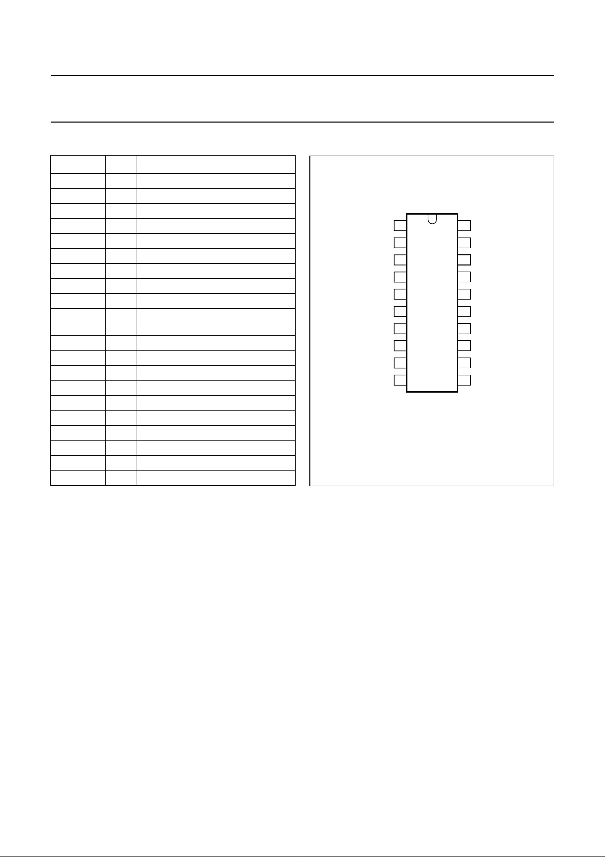
6 PINNING
SYMBOL PIN DESCRIPTION
BC 1 brightness control
VIN1 2 signal input channel 1
GC1 3 gain control channel 1
GND 4 ground
VIN2 5 signal input channel 2
CC 6 contrast control, OSD switch
V
P
7 supply voltage
VIN3 8 signal input channel 3
HBL 9 horizontal blanking, switch-off
CL 10 input clamping, vertical blanking,
test mode
GC3 11 gain control channel 3
FB3 12 feedback channel 3
VOUT3 13 voltage output channel 3
IOUT3 14 current output channel 3
FB2 15 feedback channel 2
VOUT2 16 voltage output channel 2
IOUT2 17 current output channel 2
FB1 18 feedback channel 1
VOUT1 19 voltage output channel 1
IOUT1 20 current output channel 1
handbook, halfpage
BC
VIN1
GC1
GND
VIN2
CC
V
VIN3
HBL
CL
1
2
3
4
5
TDA4882
6
7
P
8
9
10
20
19
18
17
16
15
14
13
12
11
MHA815
Fig.2 Pin configuration.
IOUT1
VOUT1
FB1
IOUT2
VOUT2
FB2
IOUT3
VOUT3
FB3
GC3
7 FUNCTIONAL DESCRIPTION
7.1 General
Figure 4 illustrates the signal processing. The RGB input
signals 0.7 V (p-p) are capacitively coupled into the
TDA4882 from a low ohmic source and are clamped to an
internal DC voltage (artificial black level). Composite
signals will not disturb normal operations because an
internal clipping circuit cuts all signal parts below black
level. Channels 1 and 3 have a maximum total voltage
gain of 7 dB (maximum contrast and maximum individual
channel gain), channel 2 having 4.4 dB (maximum
contrast and nominal gain). With the nominal channel gain
of 1 dB and nominal contrast setting the nominal
black-to-white output signal is 0.79 V (p-p). Brightness,
contrast and gain control is by DC voltage.
7.2 Brightness control
Brightness control (Fig.4) yields a simultaneous signal
black-level shift of the three channels relative to a
reference black level.
1997 Sep 04 5
For nominal brightness (pin 1 open-circuit) the signal black
level is equal to the reference black level.
7.3 Contrast control
Contrast is voltage controlled to affect the three channels
simultaneously (Fig.4). To provide the correct white point,
individual gain controls adjust the signals of channels 1
and 3 relative to the reference channel 2. Gain setting also
changes contrast to achieve correct grey scale tracking.
7.4 Output stages
The output stages provide both voltage and current
outputs. External cascode transistors reduce power
consumption of the IC and prevent breakdown of the
output transistors. Signal output currents and peaking
characteristics are determined by external components at
the voltage outputs and the video supply. The channels
have separate internal feedback loops which ensure large
signal linearity and marginal signal distortion irrespective
of output transistor thermal V
variation (Fig.8).
BE

Philips Semiconductors Product specification
Advanced monitor video controller for OSD TDA4882
7.5 Input clamping
The clamping pulse (Fig.17) is for input clamping only.
The input signals are at black level during the clamping
pulse and are clamped to an internal artificial black level.
The coupling capacitors provide black-level storage.
The threshold for the clamping pulse is higher than that for
vertical blanking, therefore, the rise and fall times of the
clamping pulse need to be faster than 75 ns/V during
transition from 1 to 3.5 V.
7.6 Vertical blanking
The vertical blanking pulse (Fig.17) will be detected if the
input voltage is higher than the threshold voltage for
approximately 320 ns but does not exceed the threshold
for the clamping pulse in the time between. During the
vertical blanking pulse the input clamping is disabled to
avoid misclamping in the event of composite input signals.
The input signal is blanked and the artificial black level is
inserted instead. Also the brightness is set internally to its
nominal value, thus the output signal is at reference black
level. The DC value of the reference black level will be
adjusted by cut-off stabilization.
7.7 Horizontal blanking
During horizontal blanking (Fig.18) the output signal is set
to reference black level and output clamping is activated.
If the voltage exceeds the switch-off threshold, the signal
is blanked and switched to ultra-black level for screen
protection and spot suppression during V-flyback.
Ultra-black level is the lowest possible channel output
voltage and is not dependent on cut-off stabilization.
7.8 Cut-off and black-level stabilization
For cut-off stabilization (DC coupling to the CRT) and
black-level stabilization (AC coupling) the video signal at
the cathode or the coupling capacitor is divided by an
adjustable voltage divider and fed to the channel feedback
inputs. During horizontal blanking time this signal is
compared with an internal DC voltage of approximately
5.8 V. Any difference will lead to a reference black-level
correction by charging or discharging the integrated
capacitor which stores the reference black-level
information between the horizontal blanking pulses.
7.9 On Screen Display
For OSD (Fig.3), fast switching of control pin 6 to less than
1 V (e.g. 0.7 V) blanks the input signals. The OSD signals
can easily be inserted to the external cascode transistor.
7.10 Test mode
During test mode (pins 9 and 10 connected to V
) the
P
black levels at the channel voltage outputs are set
internally to typical 0.7 V with nominal brightness and
3 V DC at channel signal inputs.
handbook, full pagewidth
OSD
fast blanking
1 kΩ
4.7 kΩ
100 pF
contrast
PH2222
TDA4882
6
20
17
14
Fig.3 OSD application.
1997 Sep 04 6
channel 1
channel 2
current
output
BFQ235
PH2222
150 Ω
channel 3
220 Ω
depending on
channel gain
1 kΩ to 10 kΩ
OSD
signal input
MHA816

Philips Semiconductors Product specification
Advanced monitor video controller for OSD TDA4882
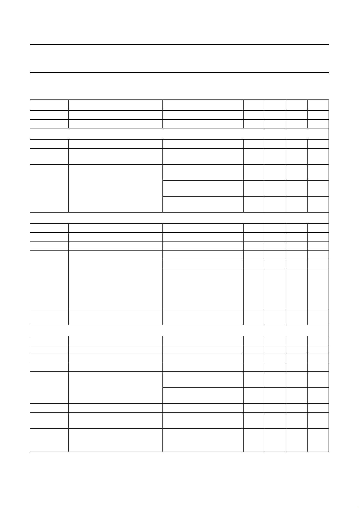
8 LIMITING VALUES
In accordance with the Absolute Maximum Rating System (IEC 134).
SYMBOL PARAMETER MIN. MAX. UNIT
V
I
o(av)
I
OM
P
T
T
T
V
ext
tot
stg
amb
j
ESD
external DC voltage applied to the following pins:
pin 7 (V
pins 2, 5 and 8 (signal inputs) −0.1 V
pins 20, 17 and 14 (current outputs) −0.1 V
) 0 8.8 V
P
P
P
V
V
pins 12, 15 and 18 (channel feedback inputs) −0.1 +0.7 V
pins 1, 6, 3 and 11 (brightness, contrast and gain control inputs) −0.1 V
pin 9 (horizontal blanking input) −0.1 V
pin 10 (input clamping input) −0.1 V
P
+ 0.7 V
P
+ 0.7 V
P
V
average output current (pins 20, 17 and 14); note 1 0 50 mA
peak output current (pins 20, 17 and 14) 0 100 mA
total power dissipation − 1200 mW
storage temperature −25 +150 °C
operating ambient temperature −20 +70 °C
junction temperature −25 +150 °C
electrostatic handling for all pins; note 2 −500 +500 V
Notes
1. Signal amplitude of 50 mA black-to-white is possible if the average current (including blanking times and signal
variation against time) does not exceed 50 mA. The maximum power dissipation of 1200 mW has to be considered.
2. Equivalent to discharging a 200 pF capacitor through a 0 Ω series resistor.
9 THERMAL CHARACTERISTICS
SYMBOL PARAMETER CONDITIONS VALUE UNIT
R
th(j-a)
thermal resistance from junction to ambient in free air 65 K/W
1997 Sep 04 7
Philips Semiconductors Product specification
Advanced monitor video controller for OSD TDA4882
10 CHARACTERISTICS
V
= 8.0 V; T
P
SYMBOL PARAMETER CONDITIONS MIN. TYP. MAX. UNIT
V
P
I
P
Video signal inputs (channels 1, 2 and 3)
V
i(b-w)
V
I(clamp)
I
I
Brightness control; note 2; Fig.5
V
i(BC)
R
i(BC)
V
i(BC)(nom)
∆V
bl
∆V
BT
=25°C; all voltages measured to GND (pin 4); note 1; see Fig.4; unless otherwise specified.
amb
supply voltage 7.2 8.0 8.8 V
supply current 36 48 60 mA
input voltage, black-to-white − 0.7 1.0 V
DC voltage during input clamping
2.8 3.1 3.4 V
(artificial black + VBE)
DC input current no clamping; Vi=V
T
= −20 to +70 °C
amb
during clamping;
V
i=VI(clamp)
+ 0.7 V
during clamping;
V
i=VI(clamp)
− 0.7 V
I(clamp)
;
−0.05 +0.05 +0.250µA
50 75 120 µA
−120 −75 −50 µA
input voltage 1.0 − 6.0 V
input resistance 40 50 60 kΩ
input voltage for nominal brightness pin 1 open-circuit 2.0 2.25 2.5 V
black-level voltage change at
voltage outputs referred to
reference black level during output
clamping (V
> 1.6 V) related
i(HBL)
V
= 1.0 V −13 −11 −9.5 %
i(BC)
V
=6.0V 303437%
i(BC)
pin 1 open-circuit −−0.8 %
to output signal amplitude with
nominal 0.7 V (p-p) input signal and
nominal contrast (V
i(CC)
= 4.3 V) for
any gain setting
difference of ∆Vbl between any two
−1.2 0 +1.2 %
channels
Contrast control; note 3; Fig.6
V
i(CC)
V
i(CC)(max)
V
i(CC)(nom)
I
i(CC)
C/C
nom
input voltage 1.0 − 6.0 V
maximum input voltage −−V
input voltage for nominal contrast note 4 − 4.3 − V
input current V
contrast relative to nominal contrast V
i(CC)
i(CC)
pins 3 and 11 open-circuit
V
i(CC)
pins 3 and 11 open-circuit
V
i(CC)(min)
∆G
track
input voltage for minimum contrast pins 3 and 11 open-circuit − 0.7 − V
tracking of output signals of
1V<V
channels 1, 2 and 3
t
df(C)
delay between leading (falling)
edges of contrast voltage and
voltage output waveforms
V
i(CC)
input fall time at pin 6:
t
f(CC)
1997 Sep 04 8
−1V
P
= 4.3 V −5 −1 −0.1 µA
= 6.0 V;
= 1.0 V;
< 6 V; note 5 − 0 0.5 dB
i(CC)
= 4.3 V to 0.7 V;
2.4 3.4 − dB
−26 −22 −19 dB
− 720ns
= 2 ns; note 6; Fig.10

Philips Semiconductors Product specification
Advanced monitor video controller for OSD TDA4882
SYMBOL PARAMETER CONDITIONS MIN. TYP. MAX. UNIT
t
dr(C)
t
f(C)
t
r(C)
Gain control (channel 1 and channel 3); note 7; Fig.7
V
i(GC)
V
i(GC)(nom)
R
i(GC)
∆G gain control difference relative to
delay between trailing edges
(rising) of contrast voltage and
voltage output waveforms
fall time of voltage output waveform 90% to 10% amplitude; input
V
= 0.7 V to 4.3 V;
i(CC)
input rise time at pin 6:
t
= 2 ns; note 6; Fig.10
r(CC)
fall time at pin 6: t
f(CC
− 15 25 ns
− 615ns
) = 2 ns;
note 6; Fig.10
rise time of voltage output
waveform
10% to 90% amplitude; input
rise time at pin 6:
t
= 2 ns; note 6; Fig.10
r(CC)
− 615ns
input voltage 1.0 − 6.0 V
input voltage for nominal gain pins 3 and 11 open-circuit 3.6 3.75 3.95 V
input resistance 44 55 66 kΩ
V
nominal gain
(channels 1 and 3 only)
V
i(CC)
i(CC)
= 4.3 V; V
= 4.3 V; V
= 6 V 2 2.6 3.3 dB
i(GC)
=1V −5.5 −5 −4.5 dB
i(GC)
Feedback input (channels 1, 2 and 3); note 8; Fig.8
V
ref(int)
I
o(FB)(max)
∆V
bl(CRT)
∆V
ref(T)
internal reference voltage 5.6 5.8 6.1 V
maximum output current during output clamping;
V
=3V
i(FB)
−500 −100 −60 nA
black-level variation at CRT note 9 0 40 200 mV
variation of V
ref(int)
in the
T
= −20 to +70 °C 0 20 50 mV
amb
temperature range
∆V
ref(int)(VP)
variation of V
with supply
ref(int)
7.2 V ≤ VP≤ 8.8 V 0 60 100 mV
voltage
Voltage outputs (channels 1, 2 and 3)
V
o(b-w)(nom)
V
blx(max)
V
bl(SO)
nominal signal output voltage
(black-to-white value)
maximum adjustable black-level
voltage
black-level voltage during
switch-off, equal to minimum
pins 3 and 11 open-circuit;
V
i(CC)
= 4.3 V; V
i(b-w)
= 0.7 V
during output clamping;
T
= −20 to +70 °C
amb
V
i(HBL)=VP
T
amb
; RO=33Ω;
= −20 to +70 °C
0.69 0.79 0.89 V
1 1.2 1.4 V
30 45 100 mV
adjustable black-level voltage
V
bl(TST)
black-level voltage during test
mode
V
i(HBL)=VP
; V
i(CL)=VP
open-circuit; Vi=V
I(clamp)
; pin 1
;
0.3 0.7 1.2 V
note 10
S/N signal-to-noise ratio note 11 − 50 44 dB
d
∆V
O(th)
bl(fl)
output thermal distortion I
black-level variation between
= 50 mA; note 12 − 0.6 1 %
o(b-w)
line frequency 30 kHz − 0.5 4.5 mV
clamping pulses
V
offset(max)
maximum offset during sync
clipping
VI<V
I(clamp)
note 13; Fig.9
;
0715mV
1997 Sep 04 9
 Loading...