

Philips TDA4858 Datasheet

INTEGRATED CIRCUITS
DATA SH EET
TDA4858
Economy Autosync Deflection
Controller (EASDC)
Product specification
Supersedes data of 1996 Jul 18
File under Integrated Circuits, IC02
1997 Oct 27

Philips Semiconductors Product specification
Economy Autosync Deflection Controller
(EASDC)
FEATURES
Concept features
• Full Horizontal (H) plus Vertical (V) autosync capability
• Completely DC controllable for analog and digital
concepts
• Excellent geometry control functions [e.g. automatic
correction of East-West (EW) parabola during
adjustment of vertical size and vertical shift]
• Flexible Switched Mode Power Supply (SMPS) function
block for feedback and feed forward converters
• X-ray protection
• Start-up and switch-off sequence for safe operation of
all power components
• Very good vertical linearity
• Internal supply voltage stabilization
• SDIP32 package.
Synchronization inputs
• Can handle all sync signals (horizontal, vertical,
composite and sync-on-video)
• Combined output for video clamping, vertical blanking
and protection blanking
• Start of video clamping pulses externally selectable.
Horizontal section
• Extremely low jitter
• Frequency locked loop for smooth catching of line
frequency
• Simple frequency preset of f
resistors
• DC controllable wide range linear picture position
• Soft start for horizontal driver.
min
and f
by external
max
Vertical section
• Vertical amplitude independent of frequency
• DC controllable picture height, picture position and
• Differential current outputs for DC coupling to vertical
EW section
• Output for DC adjustable EW parabola
• DC controllable picture width and trapezium correction
• Optional tracking of EW parabola with line frequency
• Prepared for additional DC controls of vertical linearity,
GENERAL DESCRIPTION
The TDA4858 is a high performance and efficient solution
for autosync monitors. The concept is fully DC controllable
and can be used in applications with a microcontroller and
stand-alone in rock bottom solutions.
The TDA4858 provides synchronization processing, H + V
synchronization with full autosync capability, and very
short settling times after mode changes. External power
components are given a great deal of protection. The IC
generates the drive waveforms for DC-coupled vertical
boosters such as TDA486x and TDA8351.
The TDA4858 provides extended functions e.g. as a
flexible SMPS block and an extensive set of geometry
control facilities, providing excellent picture quality.
Together with the Philips TDA488x video processor family
a very advanced system solution is offered.
TDA4858
S-correction
booster.
EW-corner, EW pin balance, EW parallelogram, vertical
focus by extended application.
ORDERING INFORMATION
TYPE
NUMBER
TDA4858 SDIP32 plastic shrink dual in-line package; 32 leads (400 mil) SOT232-1
1997 Oct 27 2
NAME DESCRIPTION VERSION
PACKAGE

Philips Semiconductors Product specification
Economy Autosync Deflection Controller
TDA4858
(EASDC)
QUICK REFERENCE DATA
SYMBOL PARAMETER MIN. TYP. MAX. UNIT
V
CC
I
CC
∆HPOS horizontal shift adjustment range −±10.5 − %
∆VAMP vertical size adjustment range 60 − 100 %
∆VPOS vertical shift adjustment range −±11.5 − %
∆VSCOR vertical S-correction adjustment range 2 − 46 %
∆V
EWPAR
∆V
EWWID
∆V
EWTRP
T
amb
supply voltage 9.2 − 16 V
supply current − 49 − mA
EW parabola adjustment range 0.15 − 3.0 V
horizontal size adjustment range 0.2 − 4.0 V
trapezium correction adjustment range −±0.5 − V
operating ambient temperature 0 − 70 °C
1997 Oct 27 3
Philips Semiconductors Product specification
Economy Autosync Deflection Controller
(EASDC)
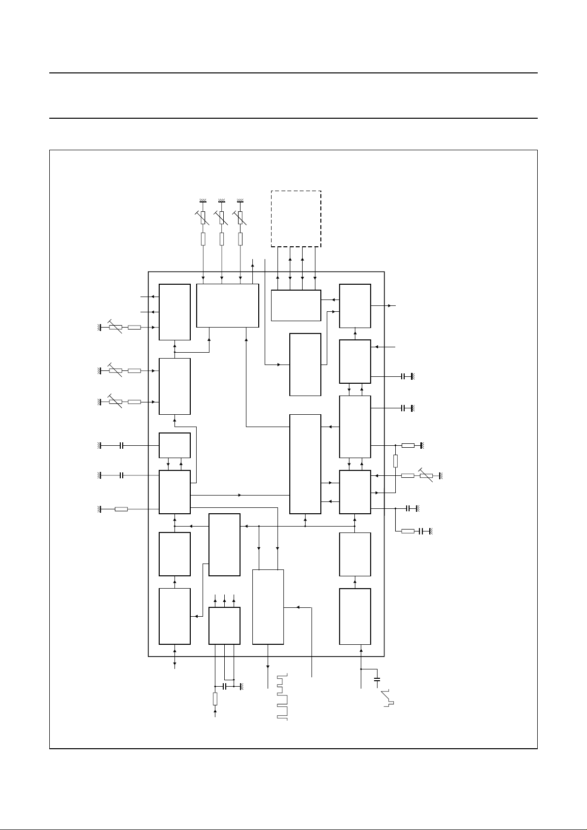
BLOCK DIAGRAM
EW
parabola
horizontal
size
EW
trapeziun
220 kΩ
220 kΩ
220 kΩ
39 kΩ
39 kΩ
39 kΩ
EWDRV
XRAY
EWPAR
EWWID
VPOS VAMP VSCOR
220 kΩ
220 kΩ
220 kΩ
100
100
22
EWTRP
21
32
20
EW
VOUT1 VOUT2
39 kΩ
39 kΩ
39 kΩ
VAGC
nF
C
5%
nF
VCAP
C
kΩ
1%
VCAP VAGC
23 24 22 17 18 19 13 12
VREF
VERTICAL
S-CORRECTION
OUTPUT STAGE
VERTICAL SIZE
VERTICAL POSITION
AGC
VERTICAL
OSCILLATOR
PARABOLA
TDA4858
BDRV
2
6
11
(2)
B+ CONTROL
APPLICATION
BSENS
BOP
BIN
4
3
5
B+
CONTROL
X-RAY
PROTECTION
FREQUENCY DETECTOR
COINCIDENCE DETECTOR
STAGE
OUTPUT
HORIZONTAL
OSCILLATOR
HORIZONTAL
PLL1 PLL2
MGD094
30 28 29 31 1 7
27
26
HCAP
HREF HPLL2
HBUF
HDRV
HFLB
12 nF
2%
10 nF
HREF
R
HBUF
R
39
1.5
TDA4858
(1)
(1)
HPOS
kΩ
kΩ
220
nF
handbook, full pagewidth
VREF
R
INTEGRATOR
POLARITY
CORRECTION
SYNC
INPUT
VERTICAL
14
VSYNC
(TTL level)
VERTICAL SYNC
AND
SUPPLY
9825
SGND
PGND
9.2 to 16 V
CC
V
REFERENCE
VERTICAL BLANKING
VIDEO CLAMPING PULSE
16
CLBL
blanking
clamping
1997 Oct 27 4
10
CLSEL
POLARITY
CORRECTION
COMPOSITE
SYNC INPUT
HORIZONTAL/
15
HSYNC
(TTL level)
(video)
HPLL1
Fig.1 Block diagram and application circuit.
47 nF
27 kΩ
range see Section “Calculation of line frequency range”.
H
(2) See Figs 12 and 13.
(1) For the calculation of f
Philips Semiconductors Product specification
Economy Autosync Deflection Controller
(EASDC)
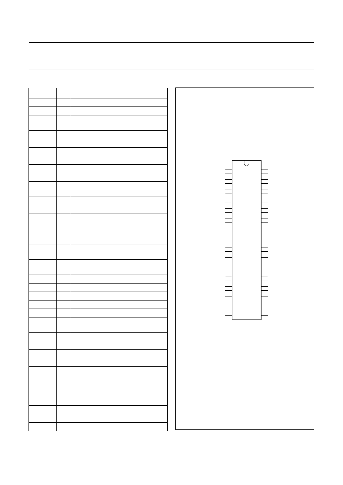
PINNING
SYMBOL PIN DESCRIPTION
HFLB 1 horizontal flyback input
XRAY 2 X-ray protection input
BOP 3 B+ control OTA output;
comparator input
BSENS 4 B+ control comparator input/output
BIN 5 B+ control OTA input
BDRV 6 B+ control driver output
HDRV 7 horizontal driver output
PGND 8 power ground
V
CC
CLSEL 10 selection input for horizontal clamping
EWDRV 11 EW parabola output
VOUT2 12 vertical output 2 (ascending sawtooth)
VOUT1 13 vertical output 1 (descending
VSYNC 14 vertical synchronization input/output
HSYNC 15 horizontal/composite synchronization
CLBL 16 video clamping pulse/vertical blanking
VPOS 17 vertical shift input
VAMP 18 vertical size input
VSCOR 19 vertical S-correction input
EWTRP 20 EW trapezium correction input
EWPAR 21 EW parabola amplitude input
VAGC 22 external capacitor for vertical
VREF 23 external resistor for vertical oscillator
VCAP 24 external capacitor for vertical oscillator
SGND 25 signal ground
HPLL1 26 external filter for PLL1
HBUF 27 buffered f/v voltage output
HREF 28 reference current for horizontal
HCAP 29 external capacitor for horizontal
HPOS 30 horizontal shift input
HPLL2 31 external filter for PLL2/soft start
EWWID 32 horizontal size input
9 supply voltage
trigger
sawtooth)
(TTL level)
input (TTL level or sync-on-video)
and protection output
amplitude control
oscillator
oscillator
handbook, halfpage
1
HFLB
2
XRAY
3
BOP
BIN
BDRV
HDRV
PGND
V
CC
CLSEL
CLBL
4
5
6
7
8
9
10
11
12
13
14
15
16
TDA4858
MGD095
BSENS
EWDRV
VOUT2
VOUT1
VSYNC
HSYNC
Fig.2 Pin configuration.
TDA4858
32
EWWID
31
HPLL2
30
HPOS
29
HCAP
28
HREF
27
HBUF
26
HPLL1
25
SGND
24
VCAP
23
VREF
22
VAGC
21
EWPAR
20
EWTRP
19
VSCOR
18
VAMP
17
VPOS
1997 Oct 27 5

Philips Semiconductors Product specification
Economy Autosync Deflection Controller
(EASDC)
FUNCTIONAL DESCRIPTION
Horizontal sync separator and polarity correction
HSYNC (pin 15) is the input for horizontal synchronization
signals, which can be DC-coupled TTL signals (horizontal
or composite sync) and AC-coupled negative-going video
sync signals. Video syncs are clamped to 1.28 V and
sliced at 1.4 V. This results in a fixed absolute slicing level
of 120 mV related to sync top.
For DC-coupled TTL signals the input clamping current is
limited. The slicing level for TTL signals is 1.4 V.
The separated sync signal (either video or TTL) is
integrated on an internal capacitor to detect and normalize
the sync polarity.
Normalized horizontal sync pulses are used as input
signals for the vertical sync integrator, the PLL1 phase
detector and the frequency-locked loop.
Vertical sync integrator
Normalized composite sync signals from HSYNC are
integrated on an internal capacitor in order to extract
vertical sync pulses. The integration time is dependent on
the horizontal oscillator reference current at HREF
(pin 28). The integrator output directly triggers the vertical
oscillator. This signal is available at VSYNC (normally
vertical sync input; pin 14), which is used as an output in
this mode.
Vertical sync slicer and polarity correction
Vertical sync signals (TTL) applied to VSYNC (pin 14) are
sliced at 1.4 V. The output signal of the sync slicer is
integrated on an internal capacitor to detect and normalize
the sync polarity.
If a composite sync signal is detected at HSYNC, VSYNC
is used as output for the integrated vertical sync (e.g. for
power saving applications).
Video clamping/vertical blanking generator
The video clamping/vertical blanking signal at CLBL
(pin 16) is a two-level sandcastle pulse which is especially
suitable for video ICs such as the TDA488x family, but also
for direct applications in video output stages.
The upper level is the video clamping pulse, which is
triggered by the trailing edge of the horizontal sync pulse.
The width of the video clamping pulse is determined by an
internal single-shot multivibrator.
TDA4858
CLSEL (pin 10) is the selection input for the position of the
video clamping pulse. If CLSEL is connected to ground,
the clamping pulse is triggered with the trailing edge of
horizontal sync. For a clamping pulse which starts with the
leading edge of horizontal sync, pin 10 must be connected
to V
.
CC
The lower level of the sandcastle pulse is the vertical
blanking pulse, which is derived directly from the internal
oscillator waveform. It is started by the vertical sync and
stopped with the start of the vertical scan. This results in
optimum vertical blanking.
Blanking will be activated continuously, if one of the
following conditions is true:
No horizontal flyback pulses at HFLB (pin 1)
X-ray protection is activated
Soft start of horizontal drive [voltage at HPLL2 (pin 31)
is LOW]
Supply voltage at VCC (pin 9) is low (see Fig.14)
PLL1 is unlocked while frequency-locked loop is in
search mode.
Blanking will not be activated if the horizontal sync
frequency is below the valid range or there are no sync
pulses available.
Frequency-locked loop
The frequency-locked loop can lock the horizontal
oscillator over a wide frequency range. This is achieved by
a combined search and PLL operation. The frequency
range is preset by two external resistors and the
f
recommended ratio is
Larger ranges are possible by extended applications.
Without a horizontal sync signal the oscillator will be
free-running at f
detected by the internal coincidence detector. A deviation
of more than 4% between horizontal sync and oscillator
frequency switches the horizontal section into search
mode. This means that PLL1 control currents are switched
off immediately. Then the internal frequency detector
starts tuning the oscillator. Very small DC currents at
HPLL1 (pin 26) are used to perform this tuning with a well
defined change rate. When coincidence between
horizontal sync and oscillator frequency is detected,
the search mode is replaced by a normal PLL operation.
min
min
---------- f
max
. Any change of sync conditions is
1
=
------- -
3.5
1997 Oct 27 6

Philips Semiconductors Product specification
Economy Autosync Deflection Controller
(EASDC)
This operation ensures a smooth tuning and avoids fast
changes of horizontal frequency during catching.
In this concept it is not allowed to load HPLL1.
The frequency dependent voltage at this pin is fed
internally to HBUF (pin 27) via a sample-and-hold and
buffer stage. The sample-and-hold stage removes all
disturbances caused by horizontal sync or composite
vertical sync from the buffered voltage. An external
resistor from HBUF to HREF defines the frequency range.
PLL1 phase detector
The phase detector is a standard type using switched
current sources. It compares the middle of horizontal sync
with a fixed point on the oscillator sawtooth voltage.
The PLL1 loop filter is connected to HPLL1 (pin 26).
Horizontal oscillator
The horizontal oscillator is of the relaxation type and
requires a capacitor of 10 nF at HCAP (pin 29).
For optimum jitter performance the value of 10 nF must not
be changed.
The maximum oscillator frequency is determined by a
resistor from HREF to ground. A resistor from HREF to
HBUF defines the frequency range.
The reference current at HREF also defines the integration
time constant of the vertical sync integration.
TDA4858
Table 1 Calculation of total spread
spread of: for f
max
IC 3% 3%
C
R
R
HCAP
HREF
HREF
, R
HBUF
2% 2%
1% −
− 1% × (2.3 × nS− 1)
Total 6% 8.69%
Thus the typical frequency range of the oscillator in this
example is:
f
maxfSmax()
f
f
min
Smin()
----------------- -
1.087
The resistors R
1.06× 67.84 kHz==
28.93 kHz==
HREF
and R
can be calculated with the
HBUF
following formulae:
R
HREF
R
HBUF
Where:
74 kHz k××Ω
-------------------------------------f
kHz[]
max
R
HREF
---------------------------------------------
n
1.18× n×
n1–
f
max
---------- f
2.35==
min
1.091 kΩ==
2.241 kΩ==
for f
min
Calculation of line frequency range
First the oscillator frequencies f
min
and f
have to be
max
calculated. This is achieved by adding the spread of the
relevant components to the highest and lowest sync
frequencies f
the difference of the currents in R
highest oscillator frequency R
S(min)
and f
. The oscillator is driven by
S(max)
and R
HREF
does not contribute to
HBUF
HBUF
. At the
the spread. The spread will increase towards lower
frequencies due to the contribution of R
f
dependent on the ratio
n
S
S max()
=
------------------f
Smin()
HBUF
. It is also
The following example is a 31.45 to 64 kHz application:
n
S
f
S max()
------------------f
Smin()
64 kHz
---------------------------
31.45 kHz
2.04== =
1997 Oct 27 7
The spread of f
f
S max()
------------------f
Smin()
increases with the frequency ratio
min
For higher ratios this spread can be reduced by using
resistors with less tolerances.

Philips Semiconductors Product specification
Economy Autosync Deflection Controller
(EASDC)
PLL2 phase detector
The PLL2 phase detector is similar to the PLL1 detector
and compares the line flyback pulse at HFLB (pin 1) with
the oscillator sawtooth voltage. The PLL2 detector thus
compensates for the delay in the external horizontal
deflection circuit by adjusting the phase of the HDRV
(pin 7) output pulse.
The phase between horizontal flyback and horizontal sync
can be controlled at HPOS (pin 30).
If HPLL2 is pulled to ground, horizontal output pulses,
vertical output currents and B+ control driver pulses are
inhibited. This means, HDRV (pin 7), BDRV (pin 6)
VOUT1 (pin 13) and VOUT2 (pin 12) are floating in this
state. PLL2 and the frequency-locked loop are disabled,
and CLBL (pin 16) provides a continuous blanking signal.
This option can be used for soft start, protection and
power-down modes. When the HPLL2 voltage is released
again, an automatic soft start sequence will be performed
(see Fig.15).
The soft start timing is determined by the filter capacitor at
HPLL2 (pin 31), which is charged with an constant current
during soft start. In the beginning the horizontal driver
stage generates very small output pulses. The width of
these pulses increases with the voltage at HPLL2 until the
final duty factor is reached. At this point BDRV (pin 6),
VOUT1 (pin 13) and VOUT2 (pin 12) are re-enabled.
The voltage at HPLL2 continues to rise until PLL2 enters
its normal operating range. The internal charge current is
now disabled. Finally PLL2 and the frequency-locked loop
are enabled, and the continuous blanking at CLBL is
removed.
Horizontal phase adjustment
HPOS (pin 30) provides a linear adjustment of the relative
phase between the horizontal sync and oscillator
sawtooth. Once adjusted, the relative phase remains
constant over the whole frequency range.
Application hint: HPOS is a current input, which provides
an internal reference voltage while I
adjustment current range. By grounding HPOS the
symmetrical control range is forced to its centre value,
therefore the phase between horizontal sync and
horizontal drive pulse is only determined by PLL2.
is in the specified
HPOS
TDA4858
Output stage for line drive pulses
An open-collector output stage allows direct drive of an
inverting driver transistor because of a low saturation
voltage of 0.3 V at 20 mA. To protect the line deflection
transistor, the output stage is disabled (floating) for low
supply voltage at V
The duty factor of line drive pulses is slightly dependent on
the actual line frequency. This ensures optimum drive
conditions over the whole frequency range.
X-ray protection
The X-ray protection input XRAY (pin 2) provides a voltage
detector with a precise threshold. If the input voltage at
XRAY exceeds this threshold for a certain time, an internal
latch switches the IC into protection mode. In this mode
several pins are forced into defined states:
Horizontal output stage (HDRV) is floating
B+ control driver stage (BDRV) is floating
Vertical output stages (VOUT1 and VOUT2) are floating
CLBL provides a continuous blanking signal
The capacitor connected to HPLL2 (pin 31) is
discharged.
To reset the latch and return to normal operation, V
to be temporarily switched off.
Vertical oscillator and amplitude control
This stage is designed for fast stabilization of vertical
amplitude after changes in sync frequency conditions.
The free-running frequency f
resistor R
connected to pin 24. The value of R
C
VCAP
connected to pin 23 and the capacitor
VREF
optimized for noise and linearity performance in the whole
vertical and EW section, but also influences several
internal references. Therefore the value of R
be changed. Capacitor C
free-running frequency of the vertical oscillator in
accordance with the following formula:
f
osc V()
=
-----------------------------------------------------------
10.8 R
To achieve a stabilized amplitude the free-running
frequency f
osc(V)
10% lower than the minimum trigger frequency.
The contributions shown in Table 2 can be assumed.
(see Fig.14).
CC
CC
is determined by the
osc(V)
is not only
VREF
must not
VREF
should be used to select the
VCAP
1
× C
VREF
×
VCAP
, without adjustment, should be at least
has
1997 Oct 27 8

Philips Semiconductors Product specification
Economy Autosync Deflection Controller
(EASDC)
Table 2 Calculation of f
Contributing elements
Minimum frequency offset between f
and lowest trigger frequency
Spread of IC ±3%
Spread of R
Spread of C
VREF
VCAP
Total 19%
Result for 50 to 110 Hz application:
f
osc V()
50 Hz
---------------
1.19
42 Hz==
Application hint: VAGC (pin 22) has a high input
impedance during scan, thus the pin must not be loaded
externally. Otherwise non-linearities in the vertical output
currents may occur due to the changing charge current
during scan.
Application hint: The full vertical sync range of 1 : 2.5 can
be made usable by incorporating an adjustment of the
free-running frequency. Also the complete sync range can
be shifted to higher frequencies (e.g. 70 to 160 Hz) by
reducing the value of C
Adjustment of vertical size, vertical shift and
S-correction
VPOS (pin 17) is the input for the DC adjustable vertical
picture shift. This pin provides a phase shift at the
sawtooth output VOUT1 and VOUT2 (pins 13 and 12) and
the EW drive output EWDRV (pin 11) in such a way, that
the whole picture moves vertically while maintaining the
correct geometry.
The amplitude of the differential output currents at VOUT1
and VOUT2 can be adjusted via input VAMP (pin 18). This
can be a combination of a DC adjustment and a dynamic
waveform modulation.
VSCOR (pin 19) is used to adjust the amount of vertical
S-correction in the output signal.
The adjustments for vertical size and vertical shift also
affect the waveforms of the EW parabola and the vertical
S-correction. The result of this interaction is that no
readjustment of these parameters is necessary after an
adjustment of vertical picture size or position.
Application hint: VPOS is a current input, which provides
an internal reference voltage while I
adjustment current range. By grounding VPOS (pin 17) the
symmetrical control range is forced to its centre value.
osc(V)
VCAP
total spread
.
VPOS
osc(V)
±10%
±1%
±5%
is in the specified
TDA4858
Application hint: VSCOR is a current input at 5 V.
Superimposed on this level is a very small positive-going
vertical sawtooth, intended to modulate an external
long-tailed transistor pair. This enables further optional DC
controls of functions which are not directly accessible such
as vertical tilt or vertical linearity (see Fig.17).
EW parabola (including horizontal size and trapezium
correction)
EWDRV (pin 11) provides a complete EW drive waveform.
EW parabola amplitude, DC shift (horizontal size) and
trapezium correction can be controlled via separate DC
inputs.
EWPAR (pin 21) is used to adjust the parabola amplitude.
This can be a combination of a DC adjustment and a
dynamic waveform modulation.
The EW parabola amplitude also tracks with vertical
picture size. The parabola waveform itself tracks with the
adjustment for vertical picture shift (VPOS).
EWWID (pin 32) offers two modes of operation:
1. Mode 1
Horizontal size is DC controlled via EWWID (pin 32)
and causes a DC shift at the EWDRV output. Also the
complete waveform is multiplied internally by a signal
proportional to the line frequency (which is detected
via the current at HREF (pin 28). This mode is to be
used for driving EW modulator stages which require a
voltage proportional to the line frequency.
2. Mode 2
EWWID (pin 32) is grounded. Then EWDRV is no
longer multiplied by the line frequency. The DC
adjustment for horizontal size must be added to the
input of the B+ control amplifier BIN (pin 5). This mode
is to be used for driving EW modulators which require
a voltage independent of the line frequency.
EWTRP (pin 20) is used to adjust the amount of trapezium
correction in the EW drive waveform.
Application hint: EWTRP (pin 20) is a current input at
5 V. Superimposed on this level is a very small vertical
parabola with positive tips, intended to modulate an
external long-tailed transistor pair. This enables further
optional DC controls of functions which are not directly
accessible such as EW-corner, vertical focus or EW pin
balance (see Fig.17).
Application hint: By grounding EWTRP (pin 20) the
symmetrical control range is forced to its centre value.
1997 Oct 27 9

Philips Semiconductors Product specification
Economy Autosync Deflection Controller
(EASDC)
B+ control function block
The B+ control function block of the EASDC consists of an
Operational Transconductance Amplifier (OTA), a voltage
comparator, a flip-flop and a discharge circuit. This
configuration allows easy applications for different
B+ control concepts.
G
ENERAL DESCRIPTION
The non-inverting input of the OTA is connected internally
to a high precision reference voltage. The inverting input is
connected to BIN (pin 5). An internal clamping circuit limits
the maximum positive output voltage of the OTA.
The output itself is connected to BOP (pin 3) and to the
inverting input of the voltage comparator.
The non-inverting input of the voltage comparator can be
accessed via BSENS (pin 4).
B+ drive pulses are generated by an internal flip-flop and
fed to BDRV (pin 6) via an open collector output stage.
This flip-flop will be set at the rising edge of the signal at
HDRV (pin 7). The falling edge of the output signal at
BDRV has a defined delay of t
the HDRV pulse. When the voltage at BSENS exceeds the
voltage at BOP, the voltage comparator output resets the
flip-flop, and therefore the open collector stage at BDRV is
floating again.
An internal discharge circuit allows a well defined
discharge of capacitors at BSENS. BDRV is active at a low
level output voltage (see Figs 12 and 13), thus it requires
an external inverting driver stage.
The B+ function block can be used for B+ deflection
modulators in either of two modes:
to the rising edge of
d(BDRV)
TDA4858
• Feedback mode (see Fig.12)
In this application the OTA is used as an error amplifier
with a limited output voltage range. The flip-flop will be
set at the rising edge of the signal at HDRV. A reset will
be generated when the voltage at BSENS taken from
the current sense resistor exceeds the voltage at BOP.
If no reset is generated within a line period, the rising
edge of the next HDRV pulse forces the flip-flop to reset.
The flip-flop is set immediately after the voltage at
BSENS has dropped below the threshold voltage
V
RESTART(BSENS)
• Feed forward mode (see Fig.13)
This application uses an external RC combination at
BSENS to provide a pulse width which is independent
from the horizontal frequency. The capacitor is charged
via an external resistor and discharged by the internal
discharge circuit. For normal operation the discharge
circuit is activated when the flip-flop is reset by the
internal voltage comparator. Now the capacitor will be
discharged with a constant current until the internally
controlled stop level V
will be maintained until the rising edge of the next HDRV
pulse sets the flip-flop again and disables the discharge
circuit.
If no reset is generated within a line period, the rising
edge of the next HDRV pulse automatically starts the
discharge sequence and resets the flip-flop (Fig.13).
When the voltage at BSENS reaches the threshold
voltage V
disabled automatically and the flip-flop will be set
immediately. This behaviour allows a definition of the
maximum duty cycle of the B+ control drive pulse by the
relationship of charge current to discharge current.
.
STOP(BSENS)
RESTART(BSENS)
is reached. This level
, the discharge circuit will be
1997 Oct 27 10

Philips Semiconductors Product specification
Economy Autosync Deflection Controller
(EASDC)
Supply voltage stabilizer, references and protection
The EASDC provides an internal supply voltage stabilizer
for excellent stabilization of all internal references.
An internal gap reference especially designed for
low-noise is the reference for the internal horizontal and
vertical supply voltages. All internal reference currents and
drive current for the vertical output stage are derived from
this voltage via external resistors.
A special protection mode has been implemented in order
to protect the deflection stages and the picture tube during
start-up, shut-down and fault conditions. This protection
mode can be activated as shown in Table 3.
Table 3 Activation of protection mode
ACTIVATION RESET
Low supply voltage at pin 9 increase supply voltage
X-ray protection XRAY (pin 2)
triggered
HPLL2 (pin 31) pulled to
ground
When protection mode is active, several pins of the ASDC
are forced into a defined state:
HDRV (horizontal driver output) is floating
BDRV (B+ control driver output) is floating
VOUT1 and VOUT2 (vertical outputs) are floating
CLBL provides a continuous blanking signal
The capacitor at HPLL2 is discharged.
remove supply voltage
release pin 31
TDA4858
If the protection mode is activated via the supply voltage at
pin 9, all these actions will be performed in a well defined
sequence (see Fig.14). For activation via X-ray protection
or HPLL2 all actions will occur simultaneously.
The return to normal operation is performed in accordance
with the start-up sequence in Fig.14a, if the reset was
caused by the supply voltage at pin 9. The first action with
increasing supply voltage is the activation of continuous
blanking at CLBL. When the threshold for activation of
HDRV is passed, an internal current begins to charge the
external capacitor at HPLL2 and a PLL2 soft start
sequence is performed (see Fig.15). In the beginning of
this phase the horizontal driver stage generates very small
output pulses. The width of these pulses increases with the
voltage at HPLL2 until the final duty cycle is reached. Then
the PLL2 voltage passes the threshold for activation of
BDRV, VOUT1 and VOUT2.
For activation of these pins not only the PLL2 voltage, but
also the supply voltage must have passed the appropriate
threshold. A last pair of thresholds has to be passed by
PLL2 voltage and supply voltage before the continuous
blanking is finally removed, and the operation of PLL2 and
frequency-locked loop is enabled.
A return to the normal operation by releasing the voltage
at HPLL2 will lead to a slightly different sequence. Here the
activation of all functions is influenced only by the voltage
at HPLL2 (see Fig.15).
Application hint: Internal discharge of the capacitor at
HPLL2 will only be performed, if the protection mode was
activated via the supply voltage or X-ray protection.
1997 Oct 27 11

Philips Semiconductors Product specification
Economy Autosync Deflection Controller
TDA4858
(EASDC)
LIMITING VALUES
In accordance with the Absolute Maximum Rating System (IEC 134); all voltages measured with respect to ground.
SYMBOL PARAMETER MIN. MAX. UNIT
V
CC
V
I(n)
V
O(n)
V
I/O(n)
I
HDRV
I
HFLB
I
CLBL
I
BOP
I
BDRV
I
EWDRV
T
amb
T
j
T
stg
V
esd
supply voltage −0.5 +16 V
input voltages
BIN −0.5 +6.0 V
HSYNC, VPOS, VAMP, VSCOR, VREF, HREF and HPOS −0.5 +6.5 V
XRAY −0.5 +8.0 V
CLSEL −0.5 +16 V
output voltages
VOUT1 and VOUT2 −0.5 +6.5 V
BDRV and HDRV −0.5 +16 V
input/output voltages
BOP and BSENS −0.5 +6.0 V
VSYNC −0.5 +6.5 V
horizontal driver output current − 100 mA
horizontal flyback input current −10 +10 mA
video clamping pulse/vertical blanking output current −−10 mA
B+ control OTA output current − 1mA
B+ control driver output current − 50 mA
EW driver output current −−5mA
operating ambient temperature 0 70 °C
junction temperature − 150 °C
storage temperature −55 +150 °C
electrostatic discharge for all pins (note 1)
machine model −400 +400 V
human body model −3000 +3000 V
Note
1. Machine model: 200 pF, 25 Ω, 2.5 µH; human body model: 100 pF, 1500 Ω, 7.5 µH.
THERMAL CHARACTERISTICS
SYMBOL PARAMETER VALUE UNIT
R
th j-a
thermal resistance from junction to ambient in free air 55 K/W
QUALITY SPECIFICATION
In accordance with
“URF-4-2-59/601”
; EMC emission/immunity test in accordance with
“DIS 1000 4.6”
(IEC 801.6)
SYMBOL PARAMETER CONDITIONS MIN. TYP. MAX. UNIT
V
EMC
emission test note 1 − 1.5 − mV
immunity test note 1 − 2.0 − V
Note
1. Tests are performed with application reference board. Tests with other boards will have different results.
1997 Oct 27 12

Philips Semiconductors Product specification
Economy Autosync Deflection Controller
TDA4858
(EASDC)
CHARACTERISTICS
V
= 12 V; T
CC
SYMBOL PARAMETER CONDITIONS MIN. TYP. MAX. UNIT
Horizontal sync separator
NPUT CHARACTERISTICS FOR DC-COUPLED TTL SIGNALS [HSYNC (PIN 15)]
I
V
DC(HSYNC)
t
r(HSYNC)
t
f(HSYNC)
t
W(HSYNC)
I
DC(HSYNC)
INPUT CHARACTERISTICS FOR AC-COUPLED VIDEO SIGNALS (SYNC-ON-VIDEO, NEGATIVE SYNC POLARITY)
V
AC(HSYNC)
V
clamp(HSYNC)
I
C(HSYNC)
t
HSYNC(min)
R
S(max)
r
diff(HSYNC)
Automatic polarity correction for horizontal sync
t
PH()
------------t
H
t
P(H)
Vertical sync integrator
t
int(V)
Vertical sync slicer (DC-coupled, TTL compatible) [VSYNC (pin 14)]
V
VSYNC
I
VSYNC
=25°C; peripheral components in accordance with Fig.1; unless otherwise specified.
amb
sync input signal voltage 1.7 −−V
slicing voltage level 1.2 1.4 1.6 V
rise time of sync pulse 10 − 500 ns
fall time of sync pulse 10 − 500 ns
minimum width of sync pulse 0.7 −−µs
input current V
V
sync amplitude of video input
= 0.8 V −−−200 µA
HSYNC
= 5.5 V −−10 µA
HSYNC
− 300 − mV
signal voltage
slicing voltage level
(measured from top sync)
source resistance
R
=50Ω
S
90 120 150 mV
top sync clamping voltage level 1.1 1.28 1.5 V
charge current for coupling
V
HSYNC
> V
clamp(HSYNC)
1.7 2.4 3.4 µA
capacitor
minimum width of sync pulse 0.7 −−µs
maximum source resistance duty factor = 7% −−1500 Ω
differential input resistance during sync − 80 −Ω
horizontal sync pulse width
related to t
H
fH< 45 kHz −−20 %
f
> 45 kHz −−25 %
H
delay time for changing polarity 0.3 − 1.8 ms
integration time for generation
of a vertical trigger pulse
fH= 31.45 kHz;
I
= 1.052 mA
HREF
f
= 64 kHz;
H
I
= 2.141 mA
HREF
= 100 kHz;
f
H
I
= 3.345 mA
HREF
71013µs
3.9 5.7 6.5 µs
2.5 3.8 4.5 µs
sync input signal voltage 1.7 −−V
slicing voltage level 1.2 1.4 1.6 V
input current 0 V < V
< 5.5 V −−±10 µA
SYNC
1997 Oct 27 13

Philips Semiconductors Product specification
Economy Autosync Deflection Controller
TDA4858
(EASDC)
SYMBOL PARAMETER CONDITIONS MIN. TYP. MAX. UNIT
VERTICAL SYNC OUTPUT AT VSYNC (PIN 14) DURING COMPOSITE SYNC AT HSYNC (PIN 15)
I
VSYNC
output current during internal vertical
sync
V
VSYNC
internal clamping voltage level during internal vertical
sync
steepness of slopes − 300 − ns/mA
Automatic polarity correction for vertical sync
t
VSYNC(max)
maximum width of vertical sync
pulse
t
d(VPOL)
delay for changing polarity 0.3 − 1.8 ms
Video clamping/vertical blanking output [CLBL (pin 16)]
t
clamp(CLBL)
V
clamp(CLBL)
width of video clamping pulse measured at V
top voltage level of video
= 3 V 0.6 0.7 0.8 µs
CLBL
clamping pulse
TC
clamp
temperature coefficient of
V
clamp(CLBL)
steepness of slopes for
R
=1MΩ; CL=20pF − 50 − ns/V
L
clamping pulse
V
blank(CLBL)
top voltage level of vertical
note 1 1.7 1.9 2.1 V
blanking pulse
t
blank(CLBL)
TC
blank
V
scan(CLBL)
width of vertical blanking pulse 240 300 360 µs
temperature coefficient of
V
blank(CLBL)
output voltage during vertical
I
= 0 0.59 0.63 0.67 V
CLBL
scan
TC
scan
I
sink(CLBL)
I
load(CLBL)
temperature coefficient of
V
scan(CLBL)
internal sink current 2.4 −−mA
external load current −−−3.0 mA
SELECTION OF LEADING/TRAILING EDGE TRIGGER FOR VIDEO CLAMPING PULSE
V
CLSEL
voltage at CLSEL (pin 10) for
trigger with leading edge of
horizontal sync
voltage at CLSEL for trigger
with trailing edge of horizontal
sync
t
d(clamp)
delay between leading edge of
V
CLSEL
>7V − 300 − ns
horizontal sync and start of
horizontal clamping pulse
delay between trailing edge of
V
CLSEL
<5V − 130 − ns
horizontal sync and start of
horizontal clamping pulse
−0.7 −1.0 −1.35 mA
4.4 4.8 5.2 V
−−300 µs
4.32 4.75 5.23 V
− +4 − mV/K
− +2 − mV/K
−−2−mV/K
7 − V
CC
0 − 5V
V
1997 Oct 27 14
 Loading...