

Philips tda4841ps DATASHEETS

INTEGRATED CIRCUITS
DATA SH EET
TDA4841PS
2
I
C-bus autosync deflection
controller for PC monitors
Product specification
File under Integrated Circuits, IC02
1999 Oct 25

Philips Semiconductors Product specification
I2C-bus autosync deflection controller for
PC monitors
FEATURES
Concept features
• Full horizontal plus vertical autosync capability
• Extended horizontal frequency range from
15 to 130 kHz
• Comprehensive set of I2C-bus driven geometry
adjustments and functions, including standby mode
• Very good vertical linearity
• Moire cancellation
• Start-up and switch-off sequence for safe operation of
all power components
• X-ray protection
• Power dip recognition
• Flexible switched mode B+ supply function block for
feedback and feed forward converter
• Internally stabilized voltage reference
• Drive signal for focus amplifiers with combined
horizontal and vertical parabola waveforms
• DC controllable inputs for Extremely High Tension
(EHT) compensation
• SDIP32 package.
Synchronization
• Can handle all sync signals (horizontal, vertical,
composite and sync-on-video)
• Output for video clamping (leading/trailing edge
selectable by I2C-bus), vertical blanking and protection
blanking
• Output for fast unlock status of horizontal
synchronization and blanking on grid 1 of picture tube.
Vertical section
• I2C-bus controllable vertical picture size, picture
• Output for I2C-bus controllable vertical sawtooth and
• Vertical picture size independent of frequency
• Differential current outputs for DC coupling to vertical
• 50 to 160 Hz vertical autosync range.
East-West (EW) section
• I2C-bus controllable output for horizontal pincushion,
• Optional tracking of EW drive waveform with line
Focus section
• I2C-bus controllable output for horizontal and vertical
• Verticalparabolaisindependentoffrequencyandtracks
• Horizontal parabola independent of frequency
• Adjustable pre-correction of delay in focus output stage.
TDA4841PS
position, linearity (S-correction) and linearity balance
parabola (for pin unbalance and parallelogram)
booster
horizontal size, corner and trapezium correction
frequency selectable by I2C-bus.
parabolas
with vertical adjustments
Horizontal section
• I2C-bus controllable wide range linear picture position,
pin unbalance and parallelogram correction via
horizontal phase
• Frequency-lockedloopforsmoothcatchingofhorizontal
frequency
• Simple frequency preset of f
resistors
• Low jitter
• Soft start for horizontal and B+ control drive signals.
1999 Oct 25 2
min
and f
by external
max
Philips Semiconductors Product specification
I2C-bus autosync deflection controller for
TDA4841PS
PC monitors
GENERAL DESCRIPTION
The TDA4841PS is a high performance and efficient
solution for autosync monitors. All functions are
controllable by the I2C-bus.
The TDA4841PS provides synchronization processing,
horizontal and vertical synchronization with full autosync
capability and very short settling times after mode
changes. External power components are given a great
deal of protection. The IC generates the drive waveforms
for DC-coupled vertical boosters such as TDA486x and
TDA835x.
QUICK REFERENCE DATA
SYMBOL PARAMETER MIN. TYP. MAX. UNIT
V
CC
I
CC
I
CC(stb)
supply voltage 9.2 − 16 V
supply current − 70 − mA
supply current during standby mode − 9 − mA
VSIZE vertical size 60 − 100 %
VGA VGA overscan for vertical size − 16.8 − %
VPOS vertical position −±11.5 − %
VLIN vertical linearity (S-correction) −2 −−46 %
VLINBAL vertical linearity balance −±1.25 − %
V
HSIZE
V
HPIN
V
HEHT
V
HTRAP
V
HCORT
V
HCORB
horizontal size voltage 0.13 − 3.6 V
horizontal pincushion voltage (EW parabola) 0.04 − 1.42 V
horizontal size modulation voltage 0.02 − 0.69 V
horizontal trapezium correction −±0.5 − V
horizontal corner correction at top of picture −0.64 − +0.2 V
horizontal corner correction at bottom of picture −0.64 − +0.2 V
HPOS horizontal position −±13 − %
HPARAL horizontal parallelogram −±1.5 − %
HPINBAL EW pin unbalance −±1.5 − %
T
amb
ambient temperature −20 − +70 °C
The TDA4841PS provides extended functions e.g. as a
flexible B+ control, an extensive set of geometry control
facilities, and a combined output for horizontal and vertical
focus signals.
Together with the I2C-bus driven Philips TDA488x video
processor family, a very advanced system solution is
offered.
ORDERING INFORMATION
TYPE
NUMBER
NAME DESCRIPTION VERSION
PACKAGE
TDA4841PS SDIP32 plastic shrink dual in-line package; 32 leads (400 mil) SOT232-1
1999 Oct 25 3
This text is here in white to force landscape pages to be rotated correctly when browsing through the pdf in the Acrobat reader.This text is here in
o
_white to force landscape pages to be rotated correctly when browsing through the pdf in the Acrobat reader.This text is here inThis text is here in
white to force landscape pages to be rotated correctly when browsing through the pdf in the Acrobat reader. white to force landscape pages to be ...
1999 Oct 25 4
k, full pagewidth
BLOCK DIAGRAM
Philips Semiconductors Product specification
PC monitors
I
2
C-bus autosync deflection controller for
clamping
blanking
HUNLOCK
V
CC
9.2 to 16 V
(TTL level)
SDA
SCL
(TTL level)
VSYNC
CLBL
PGND
SGND
HSYNC
14
VIDEO CLAMPING
16
VERTICAL BLANK
17
HUNLOCK
OUTPUT
19
18
RECEIVER
10
7
25
H/C SYNC INPUT
15
VERTICAL
SYNC INPUT
AND POLARITY
CORRECTION
AND
I2C-BUS
SUPPLY
AND
REFERENCE
AND POLARITY
CORRECTION
VERTICAL
SYNC
INTEGRATOR
HORIZONTAL
VERTICAL POSITION
VERTICAL SIZE, VOVSCN
PROTECTION
AND SOFT START
I2C-BUS REGISTERS
COINCIDENCE DETECTOR
FREQUENCY DETECTOR
PLL1 AND
POSITION
EHT compensation
via vertical size
22
100
(5%)
24
150
nF
nF
kΩ
(1%)
23 22 21 31
VERTICAL
OSCILLATOR
AND AGC
EHT compensation
via horizontal size
VSMODVAGCVCAPVREF HSMOD
EHT COMPENSATION
HORIZONTAL SIZE
AND
VERTICAL SIZE
TDA4841PS
PROTECTION
HORIZONTAL
OSCILLATOR
PLL2, PARALLELOGRAM,
PIN UNBALANCE AND
HORIZONTAL PINCUSHION
HORIZONTAL CORNER
HORIZONTAL TRAPEZIUM
HORIZONTAL SIZE
X-RAY
SOFT START
EWDRV
11
EW-OUTPUT
7 V
1.2 V
VERTICAL OUTPUT
VERTICAL LINEARITY
VERTICAL LINEARITY
BALANCE
OUTPUT
ASYMMETRIC
EW-CORRECTION
FOCUS
HORIZONTAL
AND VERTICAL
B+
CONTROL
HORIZONTAL
OUTPUT
STAGE
12
13
ASCOR
20
32 FOCUS
6
BDRV
4
BSENS
3
BOP
5
BIN
HDRV
8
VOUT2
VOUT1
or
X-RAY
B+ CONTROL
APPLICATION
(2)
(video)
3.3 kΩ
100 nF
26
R
8.2
nF
HBUF
R
HREF
(1%)
28 29
(1)
27
(1) For the calculation of fH range see Section “Calculation of line frequency range”.
(2) See Figs 25 and 26.
Fig.1 Block diagram and application circuit.
10 nF
(2%)
30 1
HPLL2HCAPHREFHBUFHPLL1
12 nF
HFLB
29
MHB603
XRAYXSEL
TDA4841PS

Philips Semiconductors Product specification
I2C-bus autosync deflection controller for
PC monitors
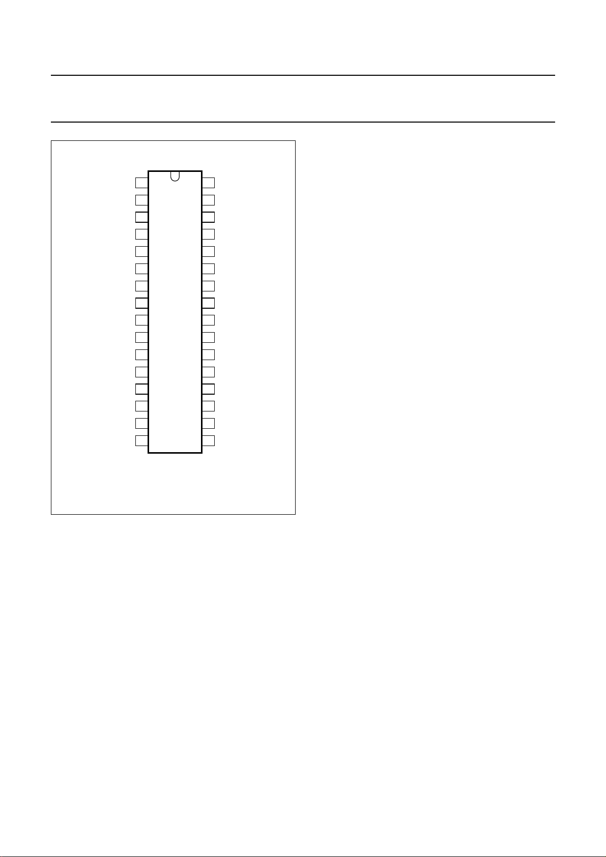
PINNING
SYMBOL PIN DESCRIPTION
HFLB 1 horizontal flyback input
XRAY 2 X-ray protection input
BOP 3 B+ control OTA output
BSENS 4 B+ control comparator input
BIN 5 B+ control OTA input
BDRV 6 B+ control driver output
PGND 7 power ground
HDRV 8 horizontal driver output
XSEL 9 select input for X-ray reset
V
CC
EWDRV 11 EW waveform output
VOUT2 12 vertical output 2 (ascending sawtooth)
VOUT1 13 vertical output 1 (descending sawtooth)
VSYNC 14 vertical synchronization input
HSYNC 15 horizontal/composite synchronization input
CLBL 16 video clamping pulse/vertical blanking output
HUNLOCK 17 horizontal synchronization unlock/protection/vertical blanking output
SCL 18 I
SDA 19 I
ASCOR 20 output for asymmetric EW corrections
VSMOD 21 input for EHT compensation (via vertical size)
VAGC 22 external capacitor for vertical amplitude control
VREF 23 external resistor for vertical oscillator
VCAP 24 external capacitor for vertical oscillator
SGND 25 signal ground
HPLL1 26 external filter for PLL1
HBUF 27 buffered f/v voltage output
HREF 28 reference current for horizontal oscillator
HCAP 29 external capacitor for horizontal oscillator
HPLL2 30 external filter for PLL2/soft start
HSMOD 31 input for EHT compensation (via horizontal size)
FOCUS 32 output for horizontal and vertical focus
10 supply voltage
2
C-bus clock input
2
C-bus data input
TDA4841PS
1999 Oct 25 5
Philips Semiconductors Product specification
I2C-bus autosync deflection controller for
PC monitors
handbook, halfpage
FUNCTIONAL DESCRIPTION
Horizontal sync separator and polarity correction
HSYNC (pin 15) is the input for horizontal synchronization
signals, which can be DC-coupled TTL signals (horizontal
or composite sync) and AC-coupled negative-going video
sync signals. Video syncs are clamped to 1.28 V and
sliced at 1.4 V. This results in a fixed absolute slicing level
of 120 mV related to sync top.
For DC-coupled TTL signals the input clamping current is
limited. The slicing level for TTL signals is 1.4 V.
The separated sync signal (either video or TTL) is
integrated on an internalcapacitor to detect and normalize
the sync polarity.
Normalized horizontal sync pulses are used as input
signals for the vertical sync integrator, the PLL1 phase
detector and the frequency-locked loop.
HFLB
1
XRAY
2
BOP
3
BSENS
EWDRV
VOUT2
VOUT1
VSYNC
HSYNC
BIN
BDRV
PGND
HDRV
XSEL
V
CC
CLBL
4
5
6
7
8
TDA4841PS
9
10
11
12
13
14
15
16
MHB604
Fig.2 Pin configuration.
FOCUS
32
HSMOD
31
HPLL2
30
HCAP
29
HREF
28
HBUF
27
HPLL1
26
SGND
25
VCAP
24
VREF
23
VAGC
22
VSMOD
21
ASCOR
20
SDA
19
SCL
18
HUNLOCK
17
TDA4841PS
Vertical sync integrator
Normalized composite sync signals from HSYNC are
integrated on an internal capacitor in order to extract
vertical sync pulses. The integration time is dependent on
the horizontal oscillator reference current at HREF
(pin 28). The integrator output directly triggers the vertical
oscillator.
Vertical sync slicer and polarity correction
Vertical sync signals (TTL) applied to VSYNC (pin 14) are
sliced at 1.4 V. The output signal of the sync slicer is
integrated on an internalcapacitor to detect and normalize
the sync polarity. The output signals of vertical sync
integrator and sync normalizer are disjuncted before they
are fed to the vertical oscillator.
Video clamping/vertical blanking generator
The video clamping/vertical blanking signal at CLBL
(pin 16) is a two-level sandcastle pulse which is especially
suitableforvideoICs such as the TDA488x family, but also
for direct applications in video output stages.
The upper level is the video clamping pulse, which is
triggered by the horizontal sync pulse. Via I2C-bus control,
either the leading or trailing edge can be selected by
settingcontrol bit CLAMP. Thewidth of the videoclamping
pulse is determined by an internal single-shot
multivibrator.
The lower level of the sandcastle pulse is the vertical
blanking pulse, which is derived directly from the internal
oscillator waveform. It is started by the vertical sync and
stopped with the start of the vertical scan. This results in
optimum vertical blanking. Via I2C-bus control, two
different vertical blanking times are accessible by control
bit VBLK.
Blanking will be activated continuously, if one of the
following conditions is true:
Soft start of horizontal and B+ drive (voltage at HPLL2
(pin 30) pulled down externally or by the I2C-bus)
PLL1 is unlocked while frequency-locked loop is in
search mode
No horizontal flyback pulses at HFLB (pin 1)
X-ray protection is activated
Supply voltage at VCC (pin 10) is low (see Fig.22).
Via I2C-bus control, horizontal unlock blanking can be
switched off by control bit BLKDIS while vertical blanking
is maintained.
1999 Oct 25 6

Philips Semiconductors Product specification
I2C-bus autosync deflection controller for
PC monitors
Frequency-locked loop
The frequency-locked loop can lock the horizontal
oscillatorover a wide frequencyrange. This is achievedby
a combined search and PLL operation. The frequency
range is preset by two external resistors and the
recommended maximum ratio is
f
----------
This can, for instance, be a range from 15.625 to 90 kHz
with all tolerances included.
Without a horizontal sync signal the oscillator will be
free-running at f
. Any change of sync conditions is
min
detected by the internal coincidence detector. A deviation
of more than 4% between horizontal sync and oscillator
frequency will switch the horizontal section into search
mode.This means that PLL1control currents are switched
off immediately. The internal frequency detector then
starts tuning the oscillator. Very small DC currents at
HPLL1 (pin 26) are used to perform this tuning with a well
defined change rate. When coincidence between
horizontal sync and oscillator frequency is detected, the
search mode is first replaced by a soft-lock mode which
lasts for the first part of the next vertical period.
The soft-lock mode is then replaced by a normal PLL
operation. This operation ensures a smooth tuning and
avoids fast changes of horizontal frequency during
catching.
In this concept it is not allowed to load HPLL1.
The frequency dependent voltage at this pin is fed
internally to HBUF (pin 27) via a sample-and-hold and
buffer stage. The sample-and-hold stage removes all
disturbances caused by horizontal sync or composite
vertical sync from the buffered voltage. An external
resistorconnectedbetween pins HBUF and HREF defines
the frequency range.
Out-of-lock indication (pin HUNLOCK)
Pin HUNLOCK is floating during search mode or if a
protection condition is true. All this can be detected by the
microcontroller if a pull-up resistor is connected to its own
supply voltage.
For an additional fast vertical blanking at grid 1 of the
picture tube, a 1 V signal referenced to ground is available
at this output. Also the continuous protection blanking
(see Section“Videoclamping/verticalblankinggenerator”)
is available at this pin. Via I2C-bus control, the control bit
BLKDIS can switch off horizontal unlock blanking while
vertical blanking is maintained.
max
f
min
6.5
=
------- 1
TDA4841PS
Horizontal oscillator
The horizontal oscillator is of the relaxation type and
requires a capacitor of 10 nF at HCAP (pin 29).
For optimum jitter performance the value of 10 nF must
not be changed.
The minimum oscillator frequency is determined by a
resistor connected between pin HREF and ground.
A resistor connected between pins HREF and HBUF
defines the frequency range.
The reference current at pin HREF also defines the
integration time constant of the vertical sync integration.
Calculation of line frequency range
First the oscillator frequencies f
calculated. This is achieved by adding the spread of the
relevant components to the highest and lowest sync
frequencies f
sync(min)
by the currents in R
and f
HREF
sync(max)
and R
Table 1 describes a 31.45 to 90 kHz application.
Table 1 Calculation of total spread
spread of for f
IC ±3% ±5%
C
R
HCAP
HREF
, R
HBUF
±2% ±2%
±2% ±2%
Total ±7% ±9%
Thus the typical frequency range of the oscillator in this
example is:
f
maxfsync max()
f
min
sync min()
-----------------------
1.09
f
The resistors R
1.07× 96.3 kHz==
28.4 kHz==
and R
HREF
HBUFpar
the following formulae:
R
HREF
R
HBUFpar
78 kHz k××Ω
----------------------------------------------------------------f
0.0012 f
min
78 kHz k××Ω
-------------------------------------------------------------------f
max
2
×+ kHz[]
min
0.0012 f
×+ kHz[]
min
and f
have to be
max
. The oscillator is driven
.
HBUF
max
for f
can be calculated with
2.61 kΩ==
2
max
726 Ω==
min
1999 Oct 25 7

Philips Semiconductors Product specification
I2C-bus autosync deflection controller for
PC monitors
The resistor R
and R
in parallel. The formulae for R
HBUF
takes into account the voltage swing across this resistor:
R
R
HBUF
HREFRHBUFpar
---------------------------------------------R
HREFRHBUFpar
PLL1 phase detector
The phase detector is a standard type using switched
current sources, which are independent of the horizontal
frequency. It compares the middle of horizontal sync with
a fixed point on the oscillator sawtooth voltage. The PLL1
loop filter is connected to HPLL1 (pin 26).
See also Section “Horizontal position adjustment and
corrections”.
Horizontal position adjustment and corrections
Via register HPOS the I
of the relative phase between the horizontal sync and
oscillator sawtooth (in PLL1 loop). Once adjusted, the
relative phase remains constant over the whole frequency
range.
Via registers HPARAL and HPINBAL correction of pin
unbalance and parallelogram is achieved by modulating
the phase between oscillator sawtooth and horizontal
flyback(in loop PLL2). If those asymmetricEWcorrections
are performed in the deflection stage, both registers can
bedisconnectedfromhorizontalphaseviacontrolbitACD.
This does not change the output at pin ASCOR.
Horizontal moire cancellation
To achieve a cancellation of horizontal moire (also known
as ‘video moire’), the horizontal frequency is
divided-by-twofor a modulation ofthe horizontal phase via
PLL2. The amplitude is controlled by register HMOIRE.
To avoid a visible structureon screen the polarity changes
with half the vertical frequency. Control bit MOD disables
the moire cancellation function.
PLL2 phase detector
The PLL2 phase detector is similar to the PLL1 detector
and compares the line flyback pulse at HFLB (pin 1) with
the oscillator sawtooth voltage. The control currents are
independent of the horizontal frequency. The PLL2
detector thus compensates for the delay in the external
horizontal deflection circuit by adjusting the phase of the
HDRV (pin 8) output pulse.
is calculated as the value of R
HBUFpar
×
–
0.8×= 805 Ω=
2
C-bus allows a linear adjustment
HBUF
HREF
additionally
TDA4841PS
An external modulation of the PLL2 phase is not allowed,
because this would disturb the pre-correction of the
H-focus parabola.
Soft start and standby
If HPLL2 is pulled to ground, either by an external DC
current or by resetting the register SOFTST, horizontal
output pulses and B+ control driver pulses are inhibited.
This means that HDRV (pin 8), BDRV (pin 6), VOUT1
(pin 13)andVOUT2(pin 12)arefloating in this state. PLL2
andthefrequency-locked loop are disabled, CLBL (pin 16)
provides a continuous blanking signal and HUNLOCK
(pin 17) is floating.
This option can be used for soft start, protection and
power-down modes. When the HPLL2 pin is released
again, an automatic soft start sequence on the horizontal
drive as well as on the B− drive output will be performed
(see Fig.22).
A soft start can only be performed if the supply voltage for
the IC is 8.6 V minimum.
The soft start timing is determined by the filter capacitor at
HPLL2 (pin 30), which is charged with an constant current
during soft start. If the voltage at pin 30 (HPLL2) reaches
1.1 V,thevertical output currents are enabled. At 1.8 Vthe
horizontaldriverstage generates very small output pulses.
The width of these pulses increases with the voltage at
HPLL2 until the final duty cycle is reached. The voltage at
HPLL2increasesfurtherandperformsa soft start at BDRV
(pin 6) as well. AfterBDRV has reachedfull duty cycle, the
voltage at HPLL2 continues to rise until HPLL2 enters its
normaloperatingrange.Theinternalchargecurrentisnow
disabled. Finally PLL2 and the frequency-locked loop are
activated. If both functions reach normal operation,
HUNLOCK (pin 17) switches from the floating status to
normal vertical blanking, andcontinuous blanking at CLBL
(pin 16) is removed.
Output stage for line drive pulses [HDRV (pin 8)]
An open-collector output stage allows direct drive of an
inverting driver transistor because of a low saturation
voltage of 0.3 V at 20 mA. To protect the line deflection
transistor, the output stage is disabled (floating) for low
supply voltage at V
The duty cycle of line drive pulses is slightly dependent on
the actual horizontal frequency. This ensures optimum
drive conditions over the whole frequency range.
(see Fig.26).
CC
1999 Oct 25 8

Philips Semiconductors Product specification
I2C-bus autosync deflection controller for
PC monitors
X-ray protection
TheX-rayprotectioninputXRAY(pin 2)providesavoltage
detector with a precise threshold. If the input voltage at
XRAY exceeds this threshold for a certain period of time,
control bit SOFTST is reset, which switches the IC into
protection mode. In this mode several pins are forced into
defined states:
HUNLOCK (pin 17) is floating
The capacitor connected to HPLL2 (pin 30) is
discharged
Horizontal output stage (HDRV) is floating
B+ control driver stage (BDRV) is floating
Vertical output stages (VOUT1 and VOUT2) are floating
CLBL provides a continuous blanking signal.
There are two different ways to restart the IC:
1. XSEL (pin 9) is open-circuit or connected to ground.
The control bit SOFTST must be set to logic 1 via the
I2C-bus. The IC then returns to normal operation via
soft start.
2. XSEL is connected to VCC via an external resistor.
The supply voltage of the IC must be switched off for a
certain time before the IC can be restartedagain using
the standard power-on procedure.
Vertical oscillator and amplitude control
This stage is designed for fast stabilization of vertical size
after changes in sync frequency conditions.
The free-running frequency f
resistor R
C
connected to pin 24. The value of R
VCAP
connected to pin 23 and the capacitor
VREF
optimized for noise and linearity performance in the whole
vertical and EW section, but also influences several
internal references. Therefore the value of R
be changed. Capacitor C
VCAP
free-running frequency of the vertical oscillator in
accordance with the following formula:
f
fr(V)
=
-----------------------------------------------------------
10.8 R
1
× C
VREF
×
To achieve a stabilized amplitude the free-running
frequencyf
,withoutadjustment,shouldbe at least 10%
fr(V)
lower than the minimum trigger frequency.
The contributions shown in Table 2 can be assumed.
is determined by the
fr(V)
VREF
VREF
should be used toselect the
VCAP
is not only
must not
TDA4841PS
Table 2 Calculation of f
Contributing elements
Minimum frequency offset between f
lowest trigger frequency
Spread of IC ±3%
Spread of R
Spread of C
VREF
VCAP
Total 19%
Result for 50 to 160 Hz application:
fr(V)
50 Hz
---------------
1.19
42 Hz==
f
The AGC of the vertical oscillator can be disabled by
setting control bit AGCDIS via the I
external current has to be injected into VCAP (pin 24) to
obtain the correct vertical size. This special application
mode can be used when the vertical sync pulses are
serrated (shifted); this condition is found in some display
modes, e.g. when using a 100 Hz upconverter for video
signals.
Application hint: VAGC (pin 22) has a high input
impedance during scan. Therefore, the pin must not be
loaded externally; otherwise non-linearities in the vertical
output currents may occur due to the changing charge
current during scan.
Adjustment of vertical size, VGA overscan and EHT compensation
There are four differentways to adjust the amplitude of the
differential output currents at VOUT1 and VOUT2:
1. Register VGAIN changes the vertical size without
affecting any other output signal of the IC; this
adjustment is meant for factory alignments.
2. Register VSIZE changes not only the vertical size, but
also provides the correct tracking of all other related
waveforms (see Section “Tracking of vertical
adjustments”); this register should be used for user
adjustments.
3. For the VGA350 mode the register VOVSCN can
activate a +17% step in vertical size.
4. VSMOD(pin 21) can be used for a DC controlled EHT
compensation of vertical size by correcting the
differential output currents at VOUT1 and VOUT2;
VSMOD does not affect the EW waveforms, vertical
focus, pin unbalance and parallelogram corrections.
total spread
fr(V)
and
fr(V)
10%
±1%
±5%
2
C-bus. A precise
1999 Oct 25 9

Philips Semiconductors Product specification
I2C-bus autosync deflection controller for
PC monitors
Adjustment of vertical position, vertical linearity and vertical linearity balance
Register VOFFS provides a DC shift at the sawtooth
output VOUT1 and VOUT2 (pins 13 and 12) without
affecting any other output waveform. This adjustment is
meant for factory alignments.
Register VPOS provides a DC shift at the sawtooth output
VOUT1 and VOUT2 with correct tracking of all other
related waveforms (see Section “Tracking of vertical
adjustments”). This register should be used for user
adjustments. Due to the tracking the whole picture moves
vertically while maintaining the correct geometry.
Register VLIN is used to adjust the amount of vertical
S-correction in the output signal. This function can be
switched off by control bit VSC.
Register VLINBAL is used to correct the unbalance of
vertical S-correction in the output signal.
Tracking of vertical adjustments
The adjustments via registers VSIZE, VOVSCN and
VPOS also affect the waveforms of horizontal pincushion,
vertical linearity (S-correction), vertical linearity balance,
focus parabola, pin unbalance and parallelogram
correction. The result of this interaction is that no
readjustment of these parameters is necessary after an
user adjustment of vertical picture size and vertical picture
position.
Adjustment of vertical moire cancellation
To achieve a cancellation of vertical moire (also known as
‘scanmoire’)theverticalpicturepositioncanbemodulated
by half the vertical frequency. The amplitude of the
modulation is controlled by register VMOIRE and can be
switched off via control bit MOD.
Horizontal pincushion (including horizontal size, corner correction and trapezium correction)
EWDRV(pin 11) provides a complete EW drive waveform.
The components horizontal pincushion, horizontal size,
corner correction and trapezium correction are controlled
by the registers HPIN, HSIZE, HCORT, HCORB and
HTRAP.
The corner correction can be adjusted separately for the
top (HCORT) and bottom (HCORB) part of the picture.
TDA4841PS
The pincushion (EW parabola) amplitude, corner and
trapezium correction track with vertical picture size
(VSIZE) and also with the adjustment for vertical picture
position(VPOS). The corner correctiondoes not track with
horizontal pincushion (HPIN).
Further the horizontal pincushion amplitude, corner and
trapezium correction track with the horizontal picture size,
which is adjusted via register HSIZE and the analog
modulation input HSMOD. If the DC component in the
EWDRV output signal is increased via HSIZE or I
the pincushion, corner and trapezium component of the
EWDRV output will be reduced by a factor of
V
HSIZE
V
+
HSIZEVHEHT
1
–
-------------------------------------------------------------------------
–
1
-----------------
14.4 V
14.4 V
The value 14.4 V is a virtual voltage for calculation only.
The output pin can not reach this value, but the gain (and
DCbias)oftheexternalapplicationshouldbesuchthatthe
horizontal deflection is reduced to zero when EWDRV
would reach 14.4 V.
HSMOD (pin 31) can be used for a DC controlled EHT
compensation by correcting horizontal size, horizontal
pincushion, corner and trapezium. The control range at
this pin tracks with the actual value of HSIZE. For an
increasing DC component V
signal, the DC component V
reducedbyafactorof asshownintheequation
1
V
–
-----------------
14.4 V
in the EWDRV output
HSIZE
caused by I
HEHT
HSIZE
above.
The whole EWDRV voltage is calculated as follows:
V
EWDRV,0
++()g HSIZE,HSMOD()⋅+
V
HPINVHCORVHTRAP
()⋅
hI
HREF
with ,
V
HEHT
g HSIZE,HSMOD()1
and
()
hI
HREF
+=
1.2 V V
I
HSMOD
------------------- 120 µA
I
=
HREF
------------------------------------ I
HREF
⋅+[
HSIZEVHEHT
f HSIZE()
0.69⋅= f HSIZE()1
V
+
HSIZEVHEHT
–=
-------------------------------------------------------------------------
f 70 kHz=
14.4 V
HSMOD
–=
–
1
HSMOD
will be
]
V
HSIZE
-----------------
14.4 V
V
HSIZE
-----------------
14.4 V
,
1999 Oct 25 10

Philips Semiconductors Product specification
I2C-bus autosync deflection controller for
PC monitors
Via control bit FHMULT two different modes of operation
can be chosen for the EW output waveform:
1. Mode 1
Horizontal size is controlled via register HSIZE and
causesaDCshift at the EWDRV output. The complete
waveform is also multiplied internally by a signal
proportional to the line frequency [which is detected
via the current at HREF (pin 28)]. This mode is to be
used for driving EW diode modulator stages which
require a voltage proportional to the line frequency.
2. Mode 2
The EW drive waveform does not track with the line
frequency. This mode is to be used for driving
EW modulators which require a voltage independent
of the line frequency.
Output stage for asymmetric correction waveforms
[ASCOR (pin 20)]
This output is designed as a voltage output for
superimposed waveforms of vertical parabola and
sawtooth. Via the I2C-bus the registers HPARAL and
HPINBAL allow to change amplitude and polarity of both
signals.
Application hint: The TDA4841PS offers two possibilities
to control HPINBAL and HPARAL.
1. Control bit ACD = 1.
The two registers now control the horizontal phase by
means of internal modulation of the PLL2 horizontal
phase control. The ASCOR output (pin 20) can be left
unused, but it will always provide an output signal
because the ASCOR output stage is not influenced by
the control bit ACD.
2. Control bit ACD = 0.
The internal modulation via PLL2 is disconnected.
In order to obtain the required effect on the screen,
pin ASCORmust now be fedtothe DC amplifier which
controls the DC shift of the horizontal deflection. This
option is useful for applications which already use a
DC shift transformer.
If the tube does not need HPINBAL and HPARAL, then
pin ASCOR can be used for other purposes, i.e. for a
simple dynamic convergence.
TDA4841PS
Dynamic focus section [FOCUS (pin 32)]
Thissectiongeneratesacompletedrivesignalfordynamic
focus applications. The amplitude of the horizontal
parabola is internally stabilized, thus it is independent of
the horizontal frequency. The amplitude can be adjusted
via register HFOCUS. Changing horizontal size may
require a correction of HFOCUS. To compensate for the
delay in external focus amplifiers a ‘pre-correction’ for the
phase of the horizontal parabola has been implemented
(see Fig.28). The amount of this pre-correction can be
adjusted via register HFOCAD. The amplitude of the
vertical parabola is independent of frequency and tracks
with all vertical adjustments. The amplitude can be
adjusted via register VFOCUS. FOCUS (pin 32) is
designedas a voltage output for thesuperimposedvertical
and horizontal parabolas.
B+ control function block
The B+ control function block of the TDA4841PS consists
of an Operational Transconductance Amplifier (OTA), a
voltagecomparator, a flip-flop and a dischargecircuit.This
configuration allows easy applications for different B+
control concepts. See also Application Note AN96052:
“B+ converter Topologies for Horizontal Deflection and
EHT with TDA4855/58”
GENERAL DESCRIPTION
The non-inverting input of the OTA is connected internally
toa high precision referencevoltage. The inverting inputis
connectedto BIN (pin 5). Aninternal clamping circuit limits
the maximum positive output voltage of the OTA.
The output itself is connected to BOP (pin 3) and to the
inverting input of the voltage comparator.
The non-inverting input of the voltage comparator can be
accessed via BSENS (pin 4).
B+ drive pulses are generated by an internal flip-flop and
fed to BDRV (pin 6) via an open-collector output stage.
This flip-flop will be set at the rising edge of the signal at
HDRV (pin 8). The falling edge of the output signal at
BDRV has a defined delay of t
theHDRV pulse. When the voltageatBSENS exceeds the
voltage at BOP, the voltage comparator output resets the
flip-flop and, therefore, the open-collector stage at BDRV
is floating again.
.
d(BDRV)
to the rising edge of
1999 Oct 25 11

Philips Semiconductors Product specification
I2C-bus autosync deflection controller for
PC monitors
An internal discharge circuit allows a well defined
discharge of capacitors at BSENS. BDRV is active at a
LOW-level output voltage (see Figs 25 and 26), thus it
requires an external inverting driver stage.
The B+ function block can be used for B+ deflection
modulators in many different ways. Two popular
application combinations are:
• Boost converter in feedback mode (see Fig.25)
In this application the OTA is used as an error amplifier
with a limited output voltage range. The flip-flop will be
set at the rising edge of the signal at HDRV. A reset will
be generated when the voltage at BSENS, taken from
the current sense resistor, exceeds the voltage at BOP.
If no reset is generated within a line period, the rising
edgeof the next HDRV pulseforces the flip-flop to reset.
The flip-flop is set immediately after the voltage at
BSENS has dropped below the threshold voltage
V
RESTART(BSENS)
• Buck converter in feed forward mode (see Fig.26)
This application uses an external RC combination at
BSENS to provide a pulse width which is independent
from the horizontal frequency. The capacitor is charged
via an external resistor and discharged by the internal
discharge circuit. For normal operation the discharge
circuit is activated when the flip-flop is reset by the
internal voltage comparator. The capacitor will now be
discharged with a constant current until the internally
controlled stop level V
willbe maintained until therising edge of thenext HDRV
pulse sets the flip-flop again and disables the discharge
circuit.
If no reset is generated within a line period, the rising
edge of the next HDRV pulse automatically starts the
discharge sequence and resets the flip-flop. When the
voltage at BSENS reaches the threshold voltage
V
RESTART(BSENS)
automatically and the flip-flop will be set immediately.
This behaviour allows a definition of the maximum duty
cycle of the B+ control drive pulse by the relationship of
charge current to discharge current.
.
STOP(BSENS)
, the discharge circuit will be disabled
is reached. This level
TDA4841PS
Supply voltage stabilizer, references, start-up procedures and protection functions
The TDA4841PS provides an internal supply voltage
stabilizer for excellent stabilization of all internal
references.Aninternalgap reference, especially designed
for low-noise, is the reference for the internal horizontal
andverticalsupplyvoltages.Allinternalreference currents
and drive current for the vertical output stage are derived
from this voltage via external resistors.
If either the supply voltage is below 8.3 V or no data from
the I2C-bus has been received after power-up, the internal
softstart and protection functions do not allowanyof those
outputs [HDRV, BDRV, VOUT1, VOUT2 and HUNLOCK
(see Fig.22)] to be active.
For supply voltages below 8.3 V the internal I2C-bus will
not generate an acknowledge and the IC is in standby
mode. This is because the internal protection circuit has
generatedaresetsignalforthe soft start register SOFTST.
Above 8.3 V data is accepted and all registers can be
loaded. If the SOFTST registerhas received a setfrom the
I2C-bus,theinternalsoftstartprocedure is released, which
activates all outputs which are mentioned above.
If during normal operation the supply voltage has dropped
below 8.1 V, the protection mode is activated and
HUNLOCK(pin 17)changesto the protection status and is
floating. This can be detected by the microprocessor.
This protection mode has been implemented in order to
protect the deflection stages and the picture tube during
start-up, shut-down and fault conditions. This protection
mode can be activated as shown in Table 3.
1999 Oct 25 12

Philips Semiconductors Product specification
I2C-bus autosync deflection controller for
PC monitors
Table 3 Activation of protection mode
ACTIVATION RESET
Low supply voltage at
pin 10
Power dip, below 8.1 V reload registers,
X-ray protection XRAY
(pin 2) triggered
HPLL2 (pin 30) externally
pulled to ground
When the protection mode is active, several pins of the
TDA4841PS are forced into a defined state:
HDRV (horizontal driver output) is floating
BDRV (B+ control driver output) is floating
HUNLOCK (indicates, that the frequency-to-voltage
converter is out of lock) is floating (HIGH via external
pull-up resistor)
CLBL provides a continuous blanking signal
VOUT1 and VOUT2 (vertical outputs) are floating
The capacitor at HPLL2 is discharged.
increase supply voltage,
reload registers,
soft start via I
soft start via I
supply voltage
reload registers,
soft start via I
release pin 30
2
C-bus
2
C-bus or via
2
C-bus
TDA4841PS
Power dip recognition
In standby mode the I2C-bus will only answer with an
acknowledgewhendataissenttothe control register 1AH.
This register contains the standby and soft start control bit.
If the I2C-bus master transmits data to another register, an
acknowledge is given after the chip address and the
subaddress; an acknowledge is not given after the data.
Thisindicates that data can bestoredinto normal registers
only in soft start mode.
If the supply voltage drops below 8.1 V the deflection
controllerleavesnormaloperationandchangestostandby
mode. The microcontroller cancheck this state by sending
data into a register with the subaddress 0XH.
The acknowledge will only be given on the data if the IC is
active.
Due to this behaviour the start-up of the TDA4841PS is
defined as follows: the first data that is transferred to the
deflection controller must be sent to the control register
with subaddress 1AH. Any other subaddress will not lead
to an acknowledge. This is a limitation in checking the
I2C-busses of the monitor during start-up.
If the soft start procedure is activated via the I2C-bus, all of
these actions will beperformed in a well defined sequence
(see Figs 22 and 23).
1999 Oct 25 13
Philips Semiconductors Product specification
I2C-bus autosync deflection controller for
TDA4841PS
PC monitors
LIMITING VALUES
In accordance with the Absolute Maximum Rating System (IEC 134); all voltages measured with respect to ground.
SYMBOL PARAMETER CONDITIONS MIN. MAX. UNIT
V
CC
V
i(n)
V
o(n)
V
I/O(n)
I
o(HDRV)
I
i(HFLB)
I
o(CLBL)
I
o(BOP)
I
o(BDRV)
I
o(EWDRV)
I
o(FOCUS)
T
amb
T
j
T
stg
V
esd
supply voltage −0.5 +16 V
input voltage
pin BIN −0.5 +6.0 V
pins HSYNC, VSYNC, VREF, HREF, VSMOD and
−0.5 +6.5 V
HSMOD
pins SDA and SCL −0.5 +8.0 V
pin XRAY −0.5 +8.0 V
output voltage
pins VOUT2, VOUT1 and HUNLOCK −0.5 +6.5 V
pins BDRV and HDRV −0.5 +16 V
input/output voltages at pins BOP and BSENS −0.5 +6.0 V
horizontal driver output current − 100 mA
horizontal flyback input current −10 +10 mA
video clamping pulse/vertical blanking output current −−10 mA
B+ control OTA output current − 1mA
B+ control driver output current − 50 mA
EW driver output current −−5mA
focus driver output current −−5mA
ambient temperature −20 +70 °C
junction temperature − 150 °C
storage temperature −55 +150 °C
electrostatic discharge for all pins note 1 −150 +150 V
note 2 −2000 +2000 V
Notes
1. Machine model: 200 pF; 0.75 µH; 10 Ω.
2. Human body model: 100 pF; 7.5 µH; 1500 Ω.
THERMAL CHARACTERISTICS
SYMBOL PARAMETER CONDITIONS VALUE UNIT
R
th(j-a)
thermal resistance from junction to ambient in free air 55 K/W
QUALITY SPECIFICATION
In accordance with
“URF-4-2-59/601”
; EMC emission/immunity test in accordance with
“DIS 1000 4.6”
(IEC 801.6).
SYMBOL PARAMETER CONDITIONS MIN. TYP. MAX. UNIT
V
EMC
emission test note 1 − 1.5 − mV
immunity test note 1 − 2.0 − V
Note
1. Tests are performed with application reference board. Tests with other boards will have different results.
1999 Oct 25 14
Philips Semiconductors Product specification
I2C-bus autosync deflection controller for
TDA4841PS
PC monitors
CHARACTERISTICS
VCC= 12 V; T
SYMBOL PARAMETER CONDITIONS MIN. TYP. MAX. UNIT
Horizontal sync separator
I
NPUT CHARACTERISTICS FOR DC-COUPLED TTL SIGNALS: PIN HSYNC
V
i(HSYNC)
V
HSYNC(sl)
t
r(HSYNC)
t
f(HSYNC)
t
W(HSYNC)(min)
I
i(HSYNC)
INPUT CHARACTERISTICS FOR AC-COUPLED VIDEO SIGNALS (SYNC-ON-VIDEO, NEGATIVE SYNC POLARITY)
V
HSYNC
V
HSYNC(AC,sl)
V
clamp(HSYNC)
I
ch(HSYNC)
t
W(HSYNC)(min)
R
source(max)
R
i(diff)(HSYNC)
Automatic polarity correction for horizontal sync
t
P(H)
---------- t
H
t
d(HPOL)
Vertical sync integrator
t
int(V)
Vertical sync slicer (DC-coupled, TTL compatible): pin VSYNC
V
i(VSYNC)
V
VSYNC(sl)
I
i(VSYNC)
=25°C; peripheral components in accordance with Fig.1; unless otherwise specified.
amb
sync input signal voltage 1.7 −−V
slicing voltage level 1.2 1.4 1.6 V
rise time of sync pulse 10 − 500 ns
fall time of sync pulse 10 − 500 ns
minimum width of sync pulse 0.7 −−µs
input current V
sync amplitude of video input
i(HSYNC)
V
i(HSYNC)
R
source
= 0.8 V −−−200 µA
= 5.5 V −−10 µA
=50Ω−300 − mV
signal voltage
slicing voltage level
R
source
=50Ω 90 120 150 mV
(measured from top sync)
top sync clamping voltage level R
charge current for coupling
V
=50Ω 1.1 1.28 1.5 V
source
i(HSYNC)>Vclamp(HSYNC)
1.7 2.4 3.4 µA
capacitor
minimum width of sync pulse 0.7 −−µs
maximum source resistance duty cycle = 7% −−1500 Ω
differential input resistance during sync − 80 −Ω
horizontal sync pulse width
related to t
H
−−25 %
delay time for changing polarity 0.3 − 1.8 ms
integration time for generation
of a vertical trigger pulse
fH= 15.625 kHz;
I
= 0.52 mA
HREF
= 31.45 kHz;
f
H
I
= 1.052 mA
HREF
f
= 64 kHz;
H
I
= 2.141 mA
HREF
f
= 100 kHz;
H
I
= 3.345 mA
HREF
14 20 26 µs
71013µs
3.9 5.7 6.5 µs
2.5 3.8 4.5 µs
sync input signal voltage 1.7 −−V
slicing voltage level 1.2 1.4 1.6 V
input current 0V<V
i(VSYNC)
< 5.5 V −−±10 µA
1999 Oct 25 15
Philips Semiconductors Product specification
I2C-bus autosync deflection controller for
TDA4841PS
PC monitors
SYMBOL PARAMETER CONDITIONS MIN. TYP. MAX. UNIT
Automatic polarity correction for vertical sync
t
VSYNC(max)
maximum width of vertical sync
pulse
t
d(VPOL)
delay time for changing polarity 0.45 − 1.8 ms
Video clamping/vertical blanking output: pin CLBL
t
clamp(CLBL)
V
clamp(CLBL)
width of video clamping pulse measured at V
top voltage level of video
clamping pulse
TC
clamp
STPS
clamp
temperature coefficient of
V
clamp(CLBL)
steepness of slopes for
clamping pulse
t
d(HSYNCt-CLBL)
delay between trailing edge of
horizontal sync and start of
video clamping pulse
t
clamp(max)
maximum duration of video
clamping pulse referenced to
end of horizontal sync
t
d(HSYNCl-CLBL)
delay between leading edge of
horizontal sync and start of
video clamping pulse
t
clamp(max)
maximum duration of video
clamping pulse referenced to
end of horizontal sync
V
blank(CLBL)
top voltage level of vertical
blanking pulse
t
blank(CLBL)
width of vertical blanking pulse
at pins CLBL and HUNLOCK
TC
blank
V
scan(CLBL)
temperature coefficient of
V
blank(CLBL)
output voltage during vertical
scan
TC
scan
I
sink(CLBL)
I
L(CLBL)
temperature coefficient of
V
scan(CLBL)
internal sink current 2.4 −−mA
external load current −−−3.0 mA
= 3 V 0.6 0.7 0.8 µs
CLBL
RL=1MΩ; CL=20pF − 50 − ns/V
clamping pulse triggered
on trailing edge of
horizontal sync;
control bit CLAMP = 0;
measured at V
CLBL
=3V
clamping pulse triggered
on leading edge of
horizontal sync;
control bit CLAMP = 1;
measured at V
CLBL
=3V
notes 1 and 2 1.7 1.9 2.1 V
control bit VBLK = 0 220 260 300 µs
control bit VBLK = 1 305 350 395 µs
I
= 0 0.59 0.63 0.67 V
CLBL
−−400 µs
4.32 4.75 5.23 V
− 4 − mV/K
− 130 − ns
−−1.0 µs
− 300 − ns
−−0.15 µs
− 2 − mV/K
−−2−mV/K
1999 Oct 25 16
Philips Semiconductors Product specification
I2C-bus autosync deflection controller for
TDA4841PS
PC monitors
SYMBOL PARAMETER CONDITIONS MIN. TYP. MAX. UNIT
Horizontal oscillator: pins HCAP and HREF
f
fr(H)
free-running frequency without
PLL1 action (for testing only)
∆f
fr(H)
spread of free-running
frequency (excluding spread of
external components)
TC
fr
temperature coefficient of
free-running frequency
f
H(max)
V
HREF
maximum oscillator frequency −−130 kHz
voltage at input for reference
current
Unlock blanking detection: pin HUNLOCK
V
scan(HUNLOCK)
V
blank(HUNLOCK)
TC
blank
TC
sink
I
sink(int)
I
L(max)
I
LI
low-level voltage of HUNLOCK saturation voltage in case
blanking level of HUNLOCK IL= 0 0.9 1 1.1 V
temperature coefficient of
V
blank(HUNLOCK)
temperature coefficient of
I
sink(HUNLOCK)
internal sink current for blanking pulses;
maximum external load current V
leakage current V
PLL1 phase comparator and frequency-locked loop: pins HPLL1 and HBUF
t
W(HSYNC)(max)
maximum width of horizontal
sync pulse (referenced to line
period)
t
lock(HPLL1)
I
ctrl(HPLL1)
V
HBUF
total lock-in time of PLL1 − 40 80 ms
control currents notes 4 and 5
buffered f/v voltage at HBUF
(pin 27)
R
R
C
HBUF
HREF
HCAP
= ∞;
= 2.4 kΩ;
= 10 nF; note 3
30.53 31.45 32.39 kHz
−−±3.0 %
−100 0 +100 10−6/K
2.43 2.55 2.68 V
−−250 mV
of locked PLL1; internal
sink current = 1 mA
−−0.9 − mV/K
− 0.15 − %/K
1.4 2.0 2.6 mA
PLL1 locked
HUNLOCK
HUNLOCK
=1V −−−2mA
= 5 V in case of
−−±5µA
unlocked PLL1 and/or
protection active
−−25 %
locked mode; level 1 − 15 −µA
locked mode; level 2 − 145 −µA
minimum horizontal
− 2.55 − V
frequency
maximum horizontal
− 0.5 − V
frequency
1999 Oct 25 17
Philips Semiconductors Product specification
I2C-bus autosync deflection controller for
TDA4841PS
PC monitors
SYMBOL PARAMETER CONDITIONS MIN. TYP. MAX. UNIT
Phase adjustments and corrections via PLL1 and PLL2
HPOS horizontal position (referenced
to horizontal period)
HPINBAL horizontal pin unbalance
correction via HPLL2
(referenced to horizontal
period)
HPARAL horizontal parallelogram
correction (referenced to
horizontal period)
HMOIRE relative modulation of
horizontal position by
1
⁄2horizontal frequency;
phase alternates with
1
⁄2vertical frequency
moire cancellation off control bit MOD = 1 − 0 − %
PLL2 phase detector: pins HFLB and HPLL2
φ
PLL2
PLL2 control (advance of
horizontal drive with respect to
middle of horizontal flyback)
I
ctrl(PLL2)
Φ
PLL2
PLL2 control current − 75 −µA
relative sensitivity of PLL2
phase shift related to horizontal
period
V
PROT(HPLL2)(max)
maximum voltage for PLL2
protection mode/soft start
I
ch(PLL2)
charge current for external
capacitor during soft start
I
dch(PLL2)
discharge current for external
capacitor during soft down
register HPOS = 0 −−13 − %
register HPOS = 127 − 0 − %
register HPOS = 255 − 13 − %
register HPINBAL = 0;
−−1.2 − %
note 6
register HPINBAL = 63;
− 1.2 − %
note 6
register HPINBAL = 32;
− 0.02 − %
note 6
register HPARAL = 0;
−−1.2 − %
note 6
register HPARAL = 63;
− 1.2 − %
note 6
register HPARAL = 32;
− 0.02 − %
note 6
register HMOIRE = 0;
− 0 − %
control bit MOD = 0
register HMOIRE = 63;
− 0.02 − %
control bit MOD = 0
maximum advance;
36 −−%
register HPINBAL = 32;
register HPARAL = 32
minimumadvance;register
− 7 − %
HPINBAL = 32; register
HPARAL = 32
− 28 − mV/%
− 4.6 − V
V
V
< 3.7 V − 1 −µA
HPLL2
< 3.7 V −−1−µA
HPLL2
1999 Oct 25 18
 Loading...