

Philips TDA4820T Datasheet

INTEGRATED CIRCUITS
DATA SH EET
TDA4820T
Sync separation circuit for video
applications
Preliminary specification
File under Integrated Circuits, IC02
June 1990

Philips Semiconductors Preliminary specification
Sync separation circuit for video applications TDA4820T
FEATURES
• Fully integrated, few external components
• Positive video input signal, capacitively coupled
• Operates with non-standard video input signals
GENERAL DESCRIPTION
The TDA4820T is a monolithic integrated circuit including
a horizontal and a vertical sync separator, offering
composite sync and vertical sync extracted from the video
signal.
• Black level clamping
• Generation of composite sync slicing level at 50% of
peak sync voltage
• Vertical sync separator with double slope integrator
• Delay time of the vertical output pulse is determined by
an external resistor
• Vertical sync generation with a slicing level at 40% of
peak sync voltage
• Output stage for composite sync
• Output stage for vertical sync
QUICK REFERENCE DATA
SYMBOL PARAMETER CONDITIONS MIN. TYP. MAX. UNIT
V
P
I
P
V
2(p-p)
V
sync(p-p)
supply voltage range (pin 1) 10.8 12 13.2 V
supply current (pin 1) − 812mA
input voltage amplitude (peak-to-peak value) 0.2 1 3 V
sync pulse input voltage amplitude (pin 2)
50 300 500 mV
(peak-to-peak value)
V
o
V
o
maximum vertical sync output voltage (pin 6) I6= −1 mA 10.0 −−V
maximum composite sync output voltage
I7= −3 mA 10.0 −−V
(pin 7)
V
o
T
amb
minimum output voltage (pins 6 and 7) I
=1mA −−0.6 V
6,7
operating ambient temperature range 0 −+70 °C
ORDERING AND PACKAGE INFORMATION
EXTENDED
TYPE NUMBER
PINS PIN POSITION MATERIAL CODE
PACKAGE
TDA4820T 8 mini-pack plastic SO8; SOT96A
Note
1. SOT96-1; 1997 January 08.
June 1990 2
(1)
Philips Semiconductors Preliminary specification
Sync separation circuit for video applications TDA4820T
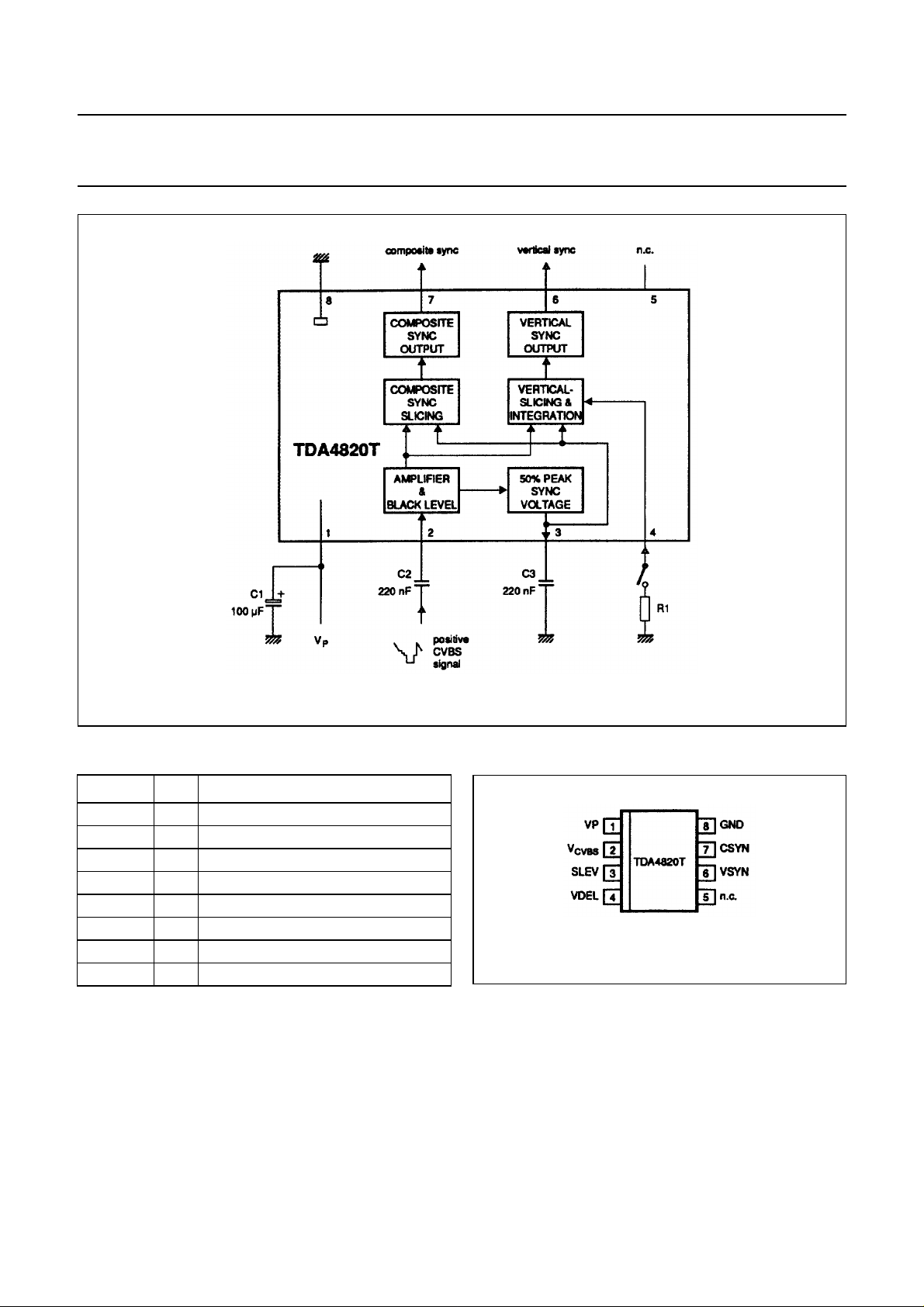
Fig.1 Block diagram and application circuit.
PINNING
SYMBOL PIN DESCRIPTION
V
P
V
CVBS
SLEV 3 slicing level
VDEL 4 vertical integration delay time
n.c. 5 not connected
VSYN 6 vertical sync output signal
CSYN 7 composite sync output signal
GND 8 ground
1 supply voltage
2 video input signal
PIN CONFIGURATION
Fig.2 Pin configuration.
June 1990 3
 Loading...