Philips tda4800 DATASHEETS

INTEGRATED CIRCUITS
DATA SH EET
TDA4800
Vertical deflection circuit for monitor
applications
Preliminary specification
File under Integrated Circuits, IC02
February 1992

Philips Semiconductors Preliminary specification
Vertical deflection circuit for monitor applications TDA4800
FEATURES
• Fully integrated, few external components
• RC oscillator with wide sync range of 1:3 (e.g. 50 Hz to
150 Hz)
• Preamplifier
• Power output stage with thermal and SOAR protection
• Flyback generator
• Internal voltage stabilizer
• Synchronization by positive or negative going sync
pulse
• Blanking pulse duration is determined externally
• Dual frequency criterion for automatic amplitude
switch-over (e.g. 50 Hz to 60 Hz)
• Guard circuit for screen protection
GENERAL DESCRIPTION
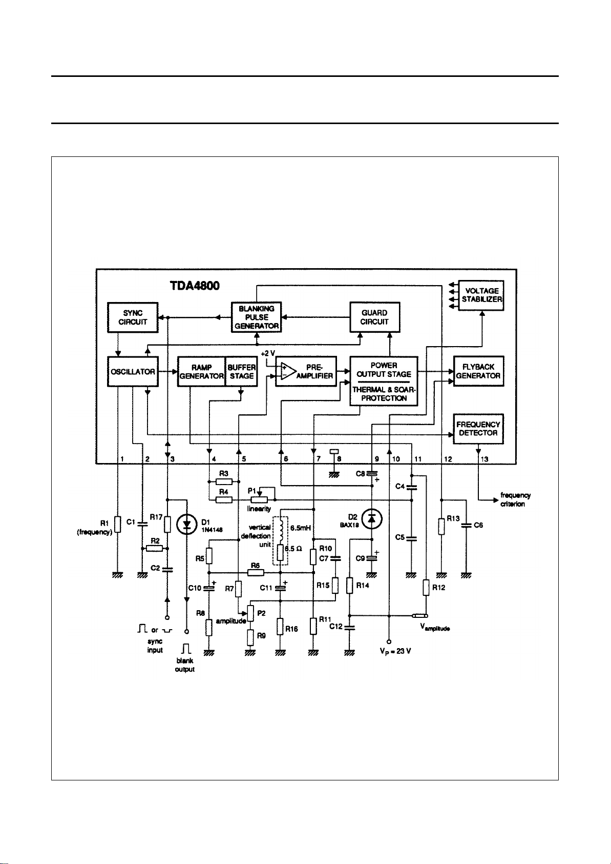
The TDA4800 is a monolithic integrated circuit for vertical
deflection primarily in monitors (and TV receivers). The
complete circuit consists of 11 main functional blocks as
shown in Fig.1.
• Sawtooth generator with buffer stage supplied by
external voltage
QUICK REFERENCE DATA
SYMBOL PARAMETER CONDITIONS MIN. TYP. MAX. UNIT
V
V
I
P
I
7
f
sync
V
V
T
P
P
3
3
amb
supply voltage range (pin 10) 10 − 45 V
supply voltage range (pin 6) 10 − 30 V
supply current (pins 6 and 10) note 1 − 215 − mA
output current (peak-to-peak value) −−2.6 A
picture frequency note 1, 3 −−135 Hz
positive sync input pulse 1.0 − 6.0 V
negative sync input pulse −0.5 −−0.7 V
operating ambient temperature range note 2 −20 −+70 °C
Notes to the quick reference data
1. Measured in circuit Fig.4
2. P
3. fo= 45 Hz (f
= 3.6 W for R
tot
sync max
th j−a
=3f
= 20 K/W
o)
ORDERING INFORMATION
EXTENDED
TYPE NUMBER
PACKAGE
PINS PIN POSITION MATERIAL CODE
TDA4800 13 DBS plastic SOT141
Note
1. SOT141-6; 1996 November 15.
February 1992 2
(1)

Philips Semiconductors Preliminary specification
Vertical deflection circuit for monitor applications TDA4800
BLOCK DIAGRAM
February 1992 3
Fig.1 Block diagram

Philips Semiconductors Preliminary specification
Vertical deflection circuit for monitor applications TDA4800
FUNCTIONAL DESCRIPTION
The complete circuit consists of the following functional
blocks as shown in Fig.1:
1. Oscillator
2. Synchronization circuit
3. Blanking pulse generator
4. Frequency detector and storage
5. Ramp generator
6. Buffer stage
7. Preamplifier
8. Power output stage
9. Flyback generator
10. Guard circuit
11. Voltage stabilizer
1. Oscillator (pins 1, 2)
The oscillator is an RC-oscillator with a threshold value
switch, which ensures very good frequency stability.
The upper and lower threshold voltages are defined by an
internal voltage divider.
An external capacitor C1 at pin 2 is charged by a constant
current source. When the scan voltage of C1 reaches the
upper threshold voltage, oscillator flyback starts. Capacitor
C1 discharges via an internal resistor and transistor until
the lower threshold is reached.
The constant charge current and free-running frequency
are adjusted by an external resistor R1 at pin 1:
f
o
f
o
1
-------------------------------KR1C1××
with K = 0.68=
2. Synchronization circuit (pin 3)
A positive- or negative-going pulse fed to pin 3
synchronizes the oscillator by lowering the upper threshold
voltage. The synchronizing range is f
50 Hz f
f
o
→ 150 Hz.==
sync max
to 3 fo. For example:
o
3. Blanking pulse generator (pin 3)
Also at pin 3 a blanking pulse is available. Diode D1
separates the synchronization pulse from the blanking
pulse. During scanning, the external capacitor C6 at pin 12
is charged to an internal stabilized voltage V. The blanking
pulse starts with the beginning of oscillator flyback; then
capacitor C6 discharges via the external resistor R13 at
pin 12. The blanking pulse stops when the capacitor
voltage is V/2.
The blanking pulse duration is determined by the values of
external components R13 and C6 at pin 12:
R13C6Ln2××=
t
bl
4. Frequency detector with storage (pin 13)
At the end of the scanning period a frequency detector
detects the oscillator frequency (see
Note
). When this
frequency is above the threshold a flip-flop is set to store
this information. The output is an open collector output.
Note:
Frequency detector change-over at pin 13 from low ( = low
frequency) to high ( = high frequency) is determined by fo:
f
threshold
1.23 fo×=
5. Ramp generator (pin 11)
The ramp generator consists of two external series
capacitors C4 and C5, external charge resistor R12
(connected to pin 11), and an internal differential amplifier
which is synchronously-switched by the oscillator.
External capacitors C4 and C5 at pin 11 are charged by
the charging current via the external charge resistor R12
until oscillator flyback starts. C4 and C5 are then
discharged via pin 11 by an internal resistor and transistor.
This generates a positive-going ramp voltage.
6. Buffer stage (pin 4)
The buffer stage consists of two emitter followers. The
ramp voltage is fed via the buffer stage and is available at
pin 4 with a low ohmic output impedance. With R4 and P1
it generates a ramp function, which, together with the
feedback network of the deflection yoke, gives a high
degree of linearity at the picture tube. The linearity can be
adjusted by P1.
7. Preamplifier (pin 5)
The preamplifier is a differential amplifier. The
non-inverting input is fixed at about 2 V by an internal
voltage divider. The inverting input at pin 5 is connected to
the ramp voltage via R3 and feedback network
P2, R5 - R11, R15, R16, C7, C10 and C11.
8. Power output stage (pin 7)
The power output stage is an amplifier with a
quasi-complementary class-B output. The output is
connected to pin 7.
The power stage includes SOAR and thermal protection.
February 1992 4
 Loading...