

Philips TDA4680WP, TDA4680 Datasheet

INTEGRATED CIRCUITS
DATA SH EET
TDA4680
Video processor with automatic
cut-off and white level control
Product specification
Supersedes data of April 1993
File under Integrated Circuits, IC02
1996 Oct 25

Philips Semiconductors Product specification
Video processor with automatic cut-off
and white level control
FEATURES
• Operates from an 8 V DC supply
• Black level clamping of the colour difference, luminance
and RGB input signals with coupling-capacitor DC level
storage
• Two fully-controlled, analog RGB inputs, selected either
by fast switch signals or via I2C-bus
• Saturation, contrast and brightness adjustment via
I2C-bus
• Same RGB output black levels for Y/CD and RGB input
signals
• Timing pulse generation from either a 2 or 3-level
sandcastle pulse for clamping, horizontal and vertical
synchronization, cut-off and white level timing pulses
• Automatic cut-off control with picture tube leakage
current compensation
• Software-based automatic white level control or fixed
white levels via I
• Cut-off and white level measurement pulses in the last
4 lines of the vertical blanking interval (I2C-bus selection
for PAL, SECAM, or NTSC, PAL-M)
• Increased RGB signal bandwidths for progressive scan
and 100 Hz operation (selected via I2C-bus)
• Two switch-on delays to prevent discolouration before
steady-state operation
• Average beam current and peak drive limiting
• PAL/SECAM or NTSC matrix selection via I2C-bus
• Three adjustable reference voltage levels (via I2C-bus)
for automatic cut-off and white level control
• Emitter-follower RGB output stages to drive the video
output stages
• Hue control output for the TDA4555, TDA4650/T,
TDA4655/T or TDA4657.
2
C-bus
TDA4680
GENERAL DESCRIPTION
The TDA4680 is a monolithic integrated circuit with a
colour difference interface for video processing in TV
receivers. Its primary function is to process the luminance
and colour difference signals from multistandard colour
decoders, TDA4555, TDA4650/T, TDA4655/T or
TDA4657, Colour Transient Improvement (CTI) IC,
TDA4565, Picture Signal Improvement (PSI) IC,
TDA4670, or from a feature module.
The required input signals are:
• Luminance and negative colour difference signals
• 2 or 3-level sandcastle pulse for internal timing pulse
generation
• I2C-bus data and clock signals for microcontroller
control.
Two sets of analog RGB colour signals can also be
inserted, e.g. one from a peritelevision connector and the
other from an on-screen display generator; both inputs are
fully-controlled internally. The TDA4680 includes full
I2C-bus control of all parameters and functions with
automatic cut-off and white level control of the picture tube
cathode currents. It provides RGB output signals for the
video output stages.
There is a very similar IC TDA4681 available. The only
differences are in the NTSC matrix.
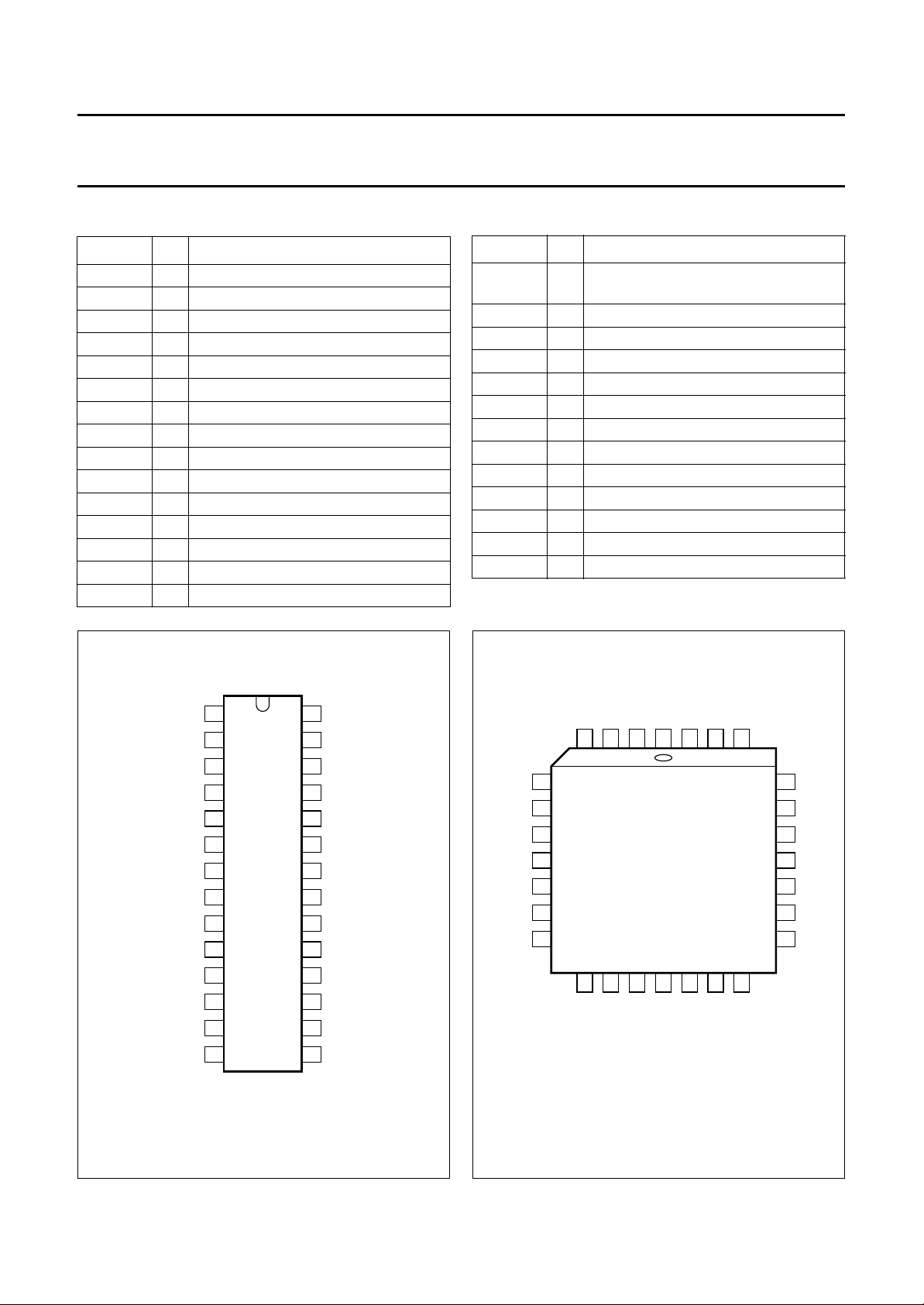
ORDERING INFORMATION
TYPE NUMBER
NAME DESCRIPTION VERSION
TDA4680 DIP28 plastic dual in-line package; 28 leads (600 mil) SOT117-1
TDA4680WP PLCC28 plastic leaded chip carrier; 28 leads SOT261-2
1996 Oct 25 2
PACKAGE

Philips Semiconductors Product specification
Video processor with automatic cut-off
TDA4680
and white level control
QUICK REFERENCE DATA
SYMBOL PARAMETER MIN. TYP. MAX. UNIT
V
P
I
P
V
8(p-p)
V
6(p-p)
V
7(p-p)
V
14
V
i(p-p)
V
o(b-w)
T
amb
supply voltage (pin 5) 7.2 8.0 8.8 V
supply current (pin 5) − 85 − mA
luminance input (peak-to-peak value) − 0.45 − V
−(B − Y) input (peak-to-peak value) − 1.33 − V
−(R − Y) input (peak-to-peak value) − 1.05 − V
3-level sandcastle pulse
H+V − 2.5 − V
H − 4.5 − V
BK − 8.0 − V
2-level sandcastle pulse
H+V − 2.5 − V
BK − 4.5 − V
RGB input signals at pins 2, 3, 4, 10, 11 and 12 (peak-to-peak value) − 0.7 − V
RGB outputs at pins 24, 22 and 20 (black-to-white value) − 2.0 − V
operating ambient temperature 0 − 70 °C
1996 Oct 25 3
Philips Semiconductors Product specification
Video processor with automatic cut-off and
white level control
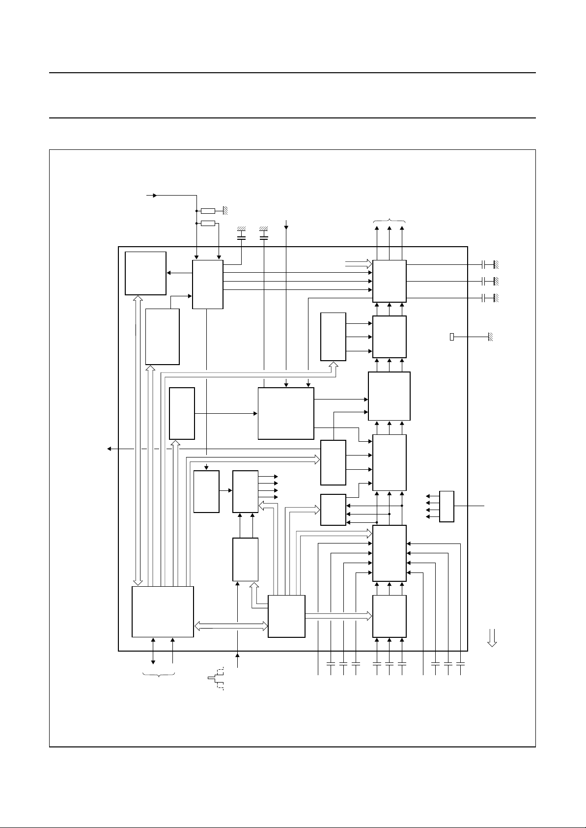
BLOCK DIAGRAM
C
R
leakage,
cut-off and
white level
current
input
AND
3 x 2-BIT
REGISTERS
WHITE LEVEL
RAR
3 x 6-BIT
cut-off
white
level
PONRES
REGISTERS,
REFERENCE
D/A CONVERTER
control
W
R
control
19
WHITE LEVEL
AND CUT-OFF
leakage
storage
18
17
COMPARATORS
peak drive
limiting
storage
16
average
15
beam
current
BCOF
D/A
3 x 6-BIT
CONVERTERS
RGB
outputs
R
G
242220
OUTPUT
ADJUST,
CUT-OFF
R
G
POINT
WHITE
ADJUST
R
G
B
STAGES
B
B
TDA4680
MED693
cut-off storage
R
GB
21 23 25
9
hue control voltage
26
PONRES, CB0 and CB1,
CG0 and CG1, CR0 and CR1
A75 to A70, A85 to A80, A95 to A90
27
SDA
6-BIT D/A
CONVERTER
DELAYS
SWITCH-ON
1ST AND 2ND
BK
A45 to A40, A55 to A50, A65 to A60
AA5 to AA0
A05 to A00, A15 to A10, A25 to A20, A35 to A30
C-BUS
2
I
TRANSCEIVER
28
SCL
C-bus
2
I
TDA4680
BREN
SANDCASTLE
14
sandcastle
pulse
AND
PEAK DRIVE
TIMING
GENERATOR
(H)
H + V
PULSE
DETECTOR
BCOF, FSBL, FSWL, WPEN,
VBW2, VBW1, VBW0
SC5
DELOF
2 x 8-BIT
LIMITING
AVERAGE
BEAM CURRENT
timing
pulses
SATOF
FSDIS2, FSON2,
NMEN
CONTROL
REGISTERS
D/A
4 x 6-BIT
CONVERTERS
Y-MATRIX
FSDIS1, FSON1
101112
13
1
1
1
R
G
FSW
1
B
ADJUST,
BLANKING 2,
BRIGHTNESS
MEASUREMENT
B
R
G
ADJUST
SATURATION
AND CONTRAST
B
R
G
BLANKING 1
FAST SIGNAL
SOURCE SWITCH,
B
R
G
NTSC
MATRIX
PAL/SECAM,
8
7
6
Y
−(R − Y)
−(B − Y)
PULSES
1
2
FSW
handbook, full pagewidth
Fig.1 Block diagram.
5
SUPPLY
2
3
4
2
2
2
B
R
G
P
V = 8 V
C-bus data and
2
control signals
I
1996 Oct 25 4
Philips Semiconductors Product specification
Video processor with automatic cut-off
and white level control
PINNING
SYMBOL PIN DESCRIPTION
FSW
2
R
2
G
2
B
2
V
P
−(B − Y) 6 colour difference input −(B − Y)
−(R − Y) 7 colour difference input −(R −Y)
Y 8 luminance input
GND 9 ground
R
1
G
1
B
1
FSW
1
SC 14 sandcastle pulse input
BCL 15 average beam current limiting input
1 fast switch 2 input
2 red input 2
3 green input 2
4 blue input 2
5 supply voltage
10 red input 1
11 green input 1
12 blue input 1
13 fast switch 1 input
TDA4680
SYMBOL PIN DESCRIPTION
C
PDL
C
L
WI 18 white level measurement input
CI 19 cut-off measurement input
B
O
C
B
G
O
C
G
R
O
C
R
HUE 26 hue control output
SDA 27 I
SCL 28 I
storage capacitor for peak drive
16
limiting
17 storage capacitor for leakage current
20 blue output
21 blue cut-off storage capacitor
22 green output
23 green cut-off storage capacitor
24 red output
25 red cut-off storage capacitor
2
C-bus serial data input/output
2
C-bus serial clock input
handbook, halfpage
FSW
R
G
B
V
−(B − Y)
−(R − Y)
GND
R
G
B
FSW
SC
2
2
2
2
P
Y
1
1
1
1
1
2
3
4
5
6
7
8
9
10
11
12
13
14
TDA4680
MED694
SCL
28
SDA
27
HUE
26
V
5
−(B − Y)
−(R − Y)
GND
R
G
P
6
7
Y
8
9
10
1
11
1
C
25
R
R
24
O
C
23
G
G
22
O
C
21
B
B
20
O
CI
19
WI
18
C
17
L
C
16
PDL
BCL
15
B2G2R2FSW2SCL
4
3
2
1
28
TDA4680WP
12
13
14
15
1
1
B
SC
FSW
16
BCLCPDL
SDA
27
17
L
C
HUE
26
18
WI
MED695
C
25
R
R
24
O
C
23
G
G
22
O
C
21
B
B
20
O
CI
19
Fig.2 Pin configuration for DIP-version.
1996 Oct 25 5
Fig.3 Pin configuration for PLCC-version.

Philips Semiconductors Product specification
Video processor with automatic cut-off
and white level control
I2C-BUS
Control
2
The I
C-bus transmitter/receiver provides the data bytes to
select and adjust the following functions and parameters:
• Brightness adjust
• Saturation adjust
• Contrast adjust
• Hue control voltage
• RGB gain adjust
• RGB reference voltage levels
• Peak drive limiting
• Selection of the vertical blanking interval and
measurement lines for cut-off and white level control
according to transmission standard
• Selects either 3-level or 2-level (5 V) sandcastle pulse
• Enables/disables input clamping pulse delay
• Enables/disables white level control
• Enables cut-off control; enables output clamping
• Enables/disables full screen white level
• Enables/disables full screen black level
• Selects either PAL/SECAM or NTSC matrix
• Enables saturation adjust; enables nominal saturation
• Enables/disables synchronization of the execution of
I2C-bus commands with the vertical blanking interval
• Reads the result of the comparison of the nominal and
actual RGB signal levels for automatic white level
control.
TDA4680
2
C-BUS RECEIVER (MICROCONTROLLER WRITE MODE)
I
Each transmission to/from the I2C-bus transceiver
consists of at least three bytes following the START bit.
Each byte is acknowledged by an acknowledge bit
immediately following each byte. The first byte is the
Module Address (MAD) byte, also called slave address
byte. This consists of the module address, 1000100 for the
TDA4680, plus the R/W bit (see Fig.4). When the
TDA4680 is a slave receiver (R/W = 0) the module
address byte is 10001000 (88H). When the TDA4680 is a
slave transmitter (R/W = 1) the module address byte is
10001001 (89H).
The length of a data transmission is unrestricted, but the
module address and the correct sub-address must be
transmitted before the data byte(s). The order of data
transmission is shown in Figs 5 and 6.
Without auto-increment (BREN = 0 or 1) the module
address (MAD) byte is followed by a Sub-Address (SAD)
byte and one data byte only (see Fig.5).
2
C-bustransmitter/receiver and data transfer
I
2
I
C-BUS SPECIFICATION
The I2C-bus is a bidirectional, two-wire, serial data bus for
intercommunication between ICs in a system.
The microcontroller transmits/receives data from the
I2C-bus transceiver in the TDA4680 over the serial data
line SDA (pin 27) synchronized by the serial clock line SCL
(pin 28). Both lines are normally connected to a positive
voltage supply through pull-up resistors. Data is
transferred when the SCL line is LOW. When SCL is HIGH
the serial data line SDA must be stable. A HIGH-to-LOW
transition of the SDA line when SCL is HIGH is defined as
a START bit. A LOW-to-HIGH transition of the SDA line
when SCL is HIGH is defined as a STOP bit.
Each transmission must start with a START bit and end
with a STOP bit. The bus is busy after a START bit and is
only free again after a STOP bit has been transmitted.
1996 Oct 25 6
Philips Semiconductors Product specification
Video processor with automatic cut-off
and white level control
handbook, full pagewidth
MSB LSB
01
module address
Fig.4 The module address byte.
TDA4680
00100
ACKX
R/W
MED696
handbook, full pagewidth
handbook, full pagewidth
STOSAD
STOP
condition
MED697
START
condition
MADSTA
data byte
Fig.5 Data transmission without auto-increment (BREN = 0 or 1).
SAD
START
condition
MADSTA
data byte
data bytes
STO
STOP
condition
MED698
Fig.6 Data transmission with auto-increment (BREN = 0).
1996 Oct 25 7

Philips Semiconductors Product specification
Video processor with automatic cut-off
and white level control
AUTO-INCREMENT
The auto-increment format enables quick slave receiver
initialization by one transmission, when the I2C-bus control
bit BREN = 0 (see control register bits of Table 1).
If BREN = 1 auto-increment is not possible.
If the auto-increment format is selected, the MAD byte is
followed by a SAD byte and by the data bytes of
consecutive sub-addresses (Fig.6).
All sub-addresses from 00H to 0FH are automatically
incremented, the sub-address counter wraps round from
0FH to 00H. Reserved sub-addresses 0BH, 0EH and 0FH
are treated as legal but have no effect. Sub-addresses
outside the range 00H and 0FH are not acknowledged by
the device and neither auto-increment nor any other
internal operation takes place (for versions V1 to V5
sub-addresses outside the range 00H and 0FH are
acknowledged but neither auto-increment nor any other
internal operation takes place).
Sub-addresses are stored in the TDA4680 to address the
following parameters and functions (see Table 1):
• Brightness adjust
• Saturation adjust
• Contrast adjust
• Hue control voltage
• RGB gain adjust
• RGB reference voltage levels
• Peak drive limiting adjust
• Control register functions.
The data bytes D7 to D0 (see Table 1) provide the data of
the parameters and functions for video processing.
ONTROL REGISTER 1
C
VBWx (Vertical Blanking Window):
x = 0, 1 or 2. VBWx selects the vertical blanking interval
and positions the measurement lines for cut-off and
white level control.
TDA4680
WPEN (White Pulse Enable):
0 = white measuring pulse disabled
1 = white measuring pulse enabled.
BREN (Buffer Register Enable):
0 = new data is executed as soon as it is received
1 = data is stored in buffer registers and is transferred to
the data registers during the next vertical blanking
interval.
2
The I
C-bus transceiver does not accept any new data
until this data is transferred into the data registers.
DELOF (Delay Off) delays the leading edge of clamping
pulses:
0 = delay enabled
1 = delay disabled.
SC5 (SandCastle 5 V):
0 = 3-level sandcastle pulse
1 = 2-level (5 V) sandcastle pulse.
C
ONTROL REGISTER 2
FSON2 (Fast Switch 2 ON)
FSDIS2 (Fast Switch 2 Disable)
FSON1 (Fast Switch 1 ON)
FSDIS1 (Fast Switch 1 Disable)
The RGB input signals are selected by FSON2 and
FSON1 or FSW2 and FSW1:
• FSON2 has priority over FSON1
• FSW2 has priority over FSW
• FSDIS1 and FSDIS2 disable FSW1 and FSW
(see Table 3).
BCOF (Black level Control Off):
0 = automatic cut-off control enabled
1 = automatic cut-off control disabled; RGB outputs are
clamped to fixed DC levels.
1
2
The actual lines in the vertical blanking interval after the
start of the vertical pulses selected as measurement lines
for cut-off and white level control are shown in Table 2.
The standards marked with (*) are for progressive line
scan at double line frequency (2fL), i.e. approximately
31 kHz.
NMEN (NTSC Matrix Enable):
0 = PAL/SECAM matrix
1 = NTSC matrix.
1996 Oct 25 8
FSBL (Full Screen Black Level):
0 = normal mode
1 = full screen black level (cut-off measurement level
during full field).
FSWL (Full Screen White Level):
0 = normal mode
1 = full screen white level (white measurement level
during full field).

Philips Semiconductors Product specification
Video processor with automatic cut-off
and white level control
SATOF (Saturation control Off):
0 = saturation control enabled
1 = saturation control disabled, nominal saturation
enabled.
2
C-BUS TRANSMITTER (MICROCONTROLLER READ MODE)
I
As an I2C-bus transmitter, R/W = 1, the TDA4680 sends a
data byte from the status register to the microcontroller.
The data byte consists of following bits: PONRES, CB1,
CB0, CG1, CG0, CR1, CR0 and 0, where PONRES is the
most significant bit.
PONRES (Power On Reset) monitors the state of
TDA4680’s supply voltage:
0 = normal operation
1 = supply voltage has dropped below approximately
6.0 V (usually occurs when the TV receiver is switched
on or the supply voltage was interrupted).
When PONRES changes state from a logic LOW to a logic
HIGH all data and function bits are set to logic LOW.
TDA4680
2-
BIT WHITE LEVEL ERROR SIGNAL (see Table 4)
CB1, CB0 = 2-bit white level of the blue channel.
CG1, CG0 = 2-bit white level of the green channel.
CR1, CR0 = 2-bit white level of the red channel.
Table 1 Sub-address (SAD) and data bytes; note 1
FUNCTION
Brightness 00 0 0 A05 A04 A03 A02 A01 A00
Saturation 01 0 0 A15 A14 A13 A12 A11 A10
Contrast 02 0 0 A25 A24 A23 A22 A21 A20
Hue control voltage 03 0 0 A35 A34 A33 A32 A31 A30
Red gain 04 0 0 A45 A44 A43 A42 A41 A40
Green gain 05 0 0 A55 A54 A53 A52 A51 A50
Blue gain 06 0 0 A65 A64 A63 A62 A61 A60
Red level reference 07 0 0 A75 A74 A73 A72 A71 A70
Green level reference 08 0 0 A85 A84 A83 A82 A81 A80
Blue level reference 09 0 0 A95 A94 A93 A92 A91 A90
Peak drive limit 0A 0 0 AA5 AA4 AA3 AA2 AA1 AA0
Reserved 0B XXXXXXXX
Control register 1 0C SC5 DELOF BREN WPEN NMEN VBW2 VBW1 VBW0
Control register 2 0D SATOF FSWL FSBL BCOF FSDIS2 FSON2 FSDIS1 FSON1
Reserved 0E XXXXXXXX
Reserved 0F XXXXXXXX
SAD
(HEX)
MSB LSB
D7 D6 D5 D4 D3 D2 D1 D0
Note
1. X = don’t care.
1996 Oct 25 9
 Loading...