

Philips tda10021 DATASHEETS
INTEGRATED CIRCUITS
DATA SH EET
TDA10021
Single Chip DVB-C Channel
Receiver
Preliminary specification
File under Integrated Circuits, IC02
2000 March 15

Philips Semiconductors Preliminary specification
Single Chip DVB-C Channel Receiver TDA10021
FEATURES
• 4/16/32/64/128/256 QAM demodulator (DVB-C compatible : ETS 300-429).
• High performance for 256 QAM especially for direct IF applications.
• On chip 10-bit ADC.
• On chip PLL for crystal frequency multiplication (Typically 4MHz crystal)
• Digital down conversion.
• Half Nyquist filter (roll off = 15 %).
• Two PWM AGC outputs with programmable take over point (For Tuner and Downconverter Control)
• Clock timing recovery, with programmable second order loop filter.
• Variable symbol rate capability from SACLK/64 to SACLK/4 (SACLK max = 36 MHz)
• Programmable anti-aliasing filters.
• Full digital carrier recovery loop.
• Carrier acquisition range up to 18 % of symbol rate.
• Integrated adaptative equalizer (Linear Transversal Equalizer or Decision Feedback Equalizer).
• On chip FEC decoder (Deinterleaver & RS decoder), full DVB-C compliant.
• DVB compatible differential decoding and mapping.
• Parallel and serial transport stream interface simultanously .
• I2C bus interface, for easy control.
• CMOS 0.2µ
m technology.
APPLICATIONS
• DVB-C fully compatible.
• Digital data transmission using QAM modulations.
• Cable demodulation.
• Cable modems
• MMDS (ETS 300-429).
DESCRIPTION
The TDA10021 is a single chip DVB-C Channel receiver for 4, 16, 32, 64, 128 and 256-Q AM modulated signals.
The device interfaces directly to the IF signal, which is sampled by a 10-bit A/D converter.
The TDA10021 performs the clock and the carrier recovery functions. The digital loop filters for both clock and
carrier recovery are programmable in order to optimize their characteristics according to the current application.
After base band conversion, equalization filters are used for echo cancellation in cable applications. These filters
are configured as T-spaced transversal equalizer or DFE equalizer, so that the system performance can be
optimized according to the network characteristics. A proprietary equalization algorithm, independent of carrier
offset, is achieved in order to assist carrier recovery. Then a decision directed algorithm takes place, to achieve
final equalization convergence.
The TDA10021 implements a FORNEY convolutional deinterleaver of depth 12 blocks and a Reed-Solomon
decoder which corrects up to 8 erroneous bytes. The deinterleaver and the RS decoder are automatically
synchronized thanks to the frame synchronization algorithm which uses the MPEG2 sync byte. Finally
descrambling according to DVB-C standard, is achieved at the Reed Solomon output. This device is controlled
via an I
Designed in 0.2 µm CMOS technology and housed in a 64 pin TQFP package, the TDA10021 operates over the
commercial temperature range.
2
C bus.
2000 March 15 2
Philips Semiconductors Preliminary specification
Single Chip DVB-C Channel Receiver TDA10021
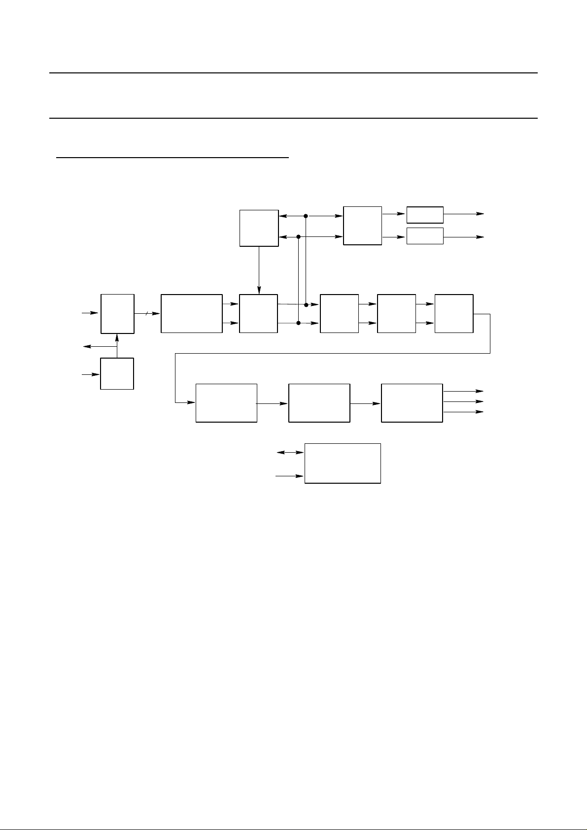
FIGURE 1 : FUNCTIONAL BLOCK DIAGRAM
IF
SACLK
XIN
ADC
PLL
10
BASE-BAND
CONVERSION
DE-INTERLEAVER
CLOCK
RECOVERY
FILTERS
BANK
SDA
SCL
EQUALIZER
R. S.
DECODER
INTERFACE
PWM
AGC
CARRIER
RECOVERY
DE-SCRAMBLER
2
IC
PWM
OUTPUT
INTERFACE
TUNER AGC
IF AGC
DO
OCLK
DEN
2000 March 15 3
Philips Semiconductors Preliminary specification
Single Chip DVB-C Channel Receiver TDA10021
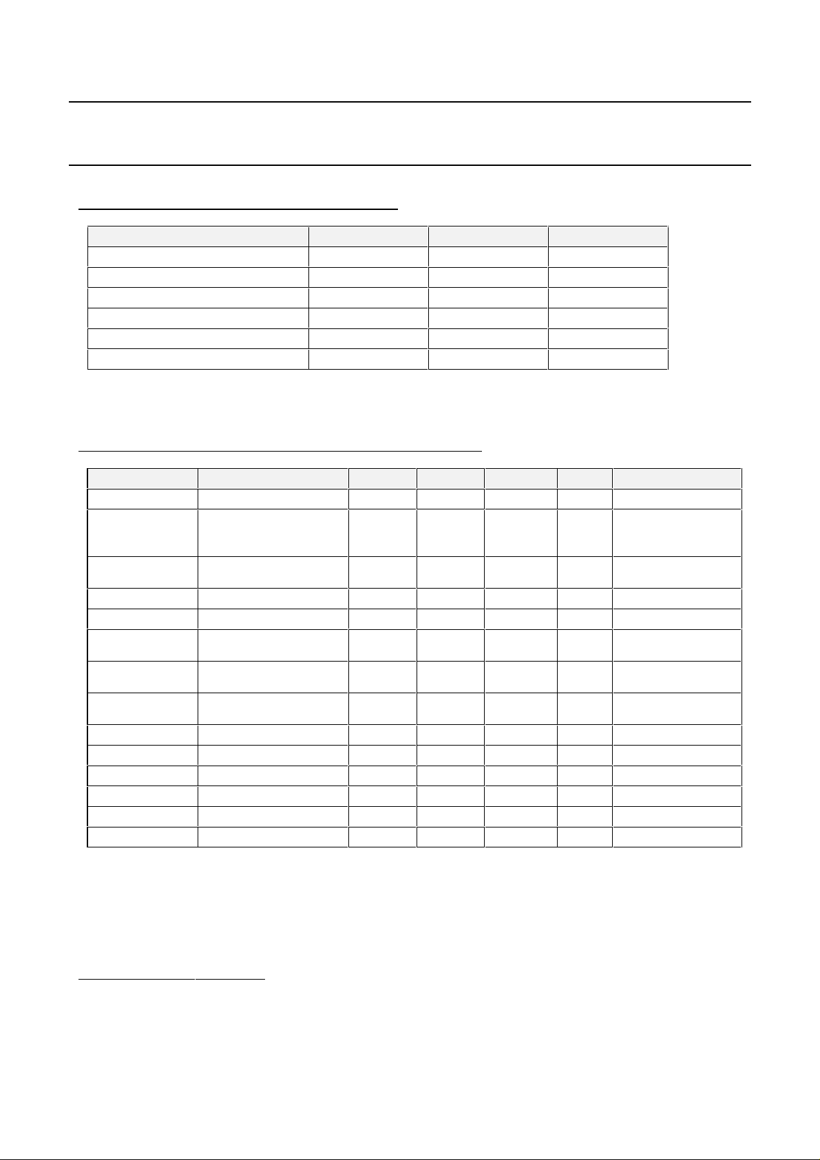
TABLE 1 : ABSOLUTE MAXIMUM RATINGS
Parameter Min Max Unit
Ambient operating temperature : Ta 0 70 °C
DC supply voltage - 0.5 Tbd V
DC Input voltage - 0.5 VDD + 0.5 V
DC Input Current ± 20 mA
Lead Temperature +300 °C
Junction Temperature +150 °C
Stresses above the absolute maximum ratings may cause permanent damage to the device. Exposure to absolute
maximum ratings conditions for extended periods may affect device reliability.
TABLE 2 : RECOMMENDED OPERATING CONDITIONS
Symbol Parameter Min Typ Max Unit Notes
VDD Digital supply voltage 1.62 1.8 1.98 V 1.8V ±10%
VCC 5V supply 4.75 5 5.25 V pin 13
Only for 5V
requirements
Ta Operating temperature 0 70 °C Ambient
1
VIH
High-level input voltage 2 VCC + 0.3 V TTL input
VIL Low-level input voltage -0.5 0.8 V TTL input
2
VOH
VOL
2
High-level output
voltage
VDD -0.1
2.4
Low-level output voltage 0.1
V @ IOH = -0.8 mA
V @ IOL = 0.8 mA
0.4
IDD Supply current t.b.d mA Fsampl. = 57.84Mhz
CIN Input capacitance t.b.d pF
COUT Output capacitance t.b.d pF
VD1 Analog supply voltage 1.6 1.8 2.0 V 1.8V ± 10%
VD2, VD3 Analog supply voltage 3.0 3.3 3.6 V 3.3V ± 10%
VIP Positive analog input 0.5 V
VIM Negative analog input -0.5 V
temperature
@ IOH = + 2mA
@ IOL = + 2mA
Symbol Rate =6Mbd
1
All inputs are 5V tolerant
2
IOH, IOL = ± 4mA only for pins SACLK, OCLK, SDA, CTRL1, CTRL2, IT
2000 March 15 4

Philips Semiconductors Preliminary specification
Single Chip DVB-C Channel Receiver TDA10021
FUNCTIONAL DESCRIPTION
ADC
½
The TDA10021 implements a 10-bit analog to digital converter. No external voltage references are required to
use the ADC.
PLL
½
The TDA10021 implements a PLL used as clock multiplier by [M/(N.P)] (programmable parameters in index 28
, 2A16), so that the crystal can be low frequency (fundamental tone – typically 4Mhz )
29
16
DOWN CONVERTER AND NYQUIST FILTERS
½
The digital down converter performs the down conversion of the bandpass input signal into the 2 classical
quadrature I & Q channels. Then these two signals are passed through anti-alias filters and through a half
Nyquist filter having a fixed roll-off of 0.15. The digital filter gives a stop band attenuation of more than 40 dB.
EQUALIZER
½
After Nyquist filtering, the signal is fed to an equalization filter, for echo cancellation. This equalizer can be
configured as either a transversal Equalizer or a decision feedback equalizer. The following table shows some
echos configuration that the TDA10021 corrects with an equivalent degradation of less than 1dB @ BER = 10
,
16
-4
.
DELAY
(nS)
AMPLITUDE
(dB)
PHASE
50 -10 worst
150
and
800
-12
and
-20
worst
1600 -20 worst
CARRIER RECOVERY
½
The carrier synchronizer implements a fully digital algorithm allowing to recover carrier frequency offsets up to
± 18 % symbol rate. A phase error detector followed by a programmable second order loop filter provides an
estimation of the carrier phase, to compensate the input carrier frequency offset.
CLOCK RECOVERY
½
A timing error detector implements an application of Gardner algorithm for digital clock recovery.
The resulting error is fed to a programmable second order loop filter, which provides a 8-bit command to the
NCO block. This one allows to determine the right sampling time instant of the input signal.
AUTOMATIC GAIN CONTROL (2 PWM outputs)
½
An estimation of input signal magnitude is performed and compared to two programmable threshold. The
resulting errors are filtered to produce two 10-bit commands which are then PWM encoded and provided on pins
VAGC1 and VAGC2. The PWM signals can be passed through two low pass filters to control the gain amplifier.
½ OUTPUT INTERFACE
After carrier recovery, the demodulated output symbol must be decoded according to the constellation diagram
given by DVB standard for 4, 16, 32, 64, 128 and 256 QAM. The resulting symbols are then differentially
decoded (DVB compliant) and serially provided to the FEC part.
½ BLOCK SYNCHRONIZATION
At demodulator output, the length of some error bursts may exceed that which can be reliably corrected by the
Reed-Solomon decoder. The implemented de-interleaving is a convolutional one (Forney) of depth 12. The first
operation consists in synchronizing the de-interleaver. This is accomplished by detecting α consecutive MPEG2
sync
sync words (or
) which are present as the first byte of each packet.
Next, the RAM memory associated with the deinterleaver fills up and the first deinterleaved bytes ar e pr ovided to
the input of the Reed-Solomon decoder. The state machine of the de-interleaver goes to the control phase which
2000 March 15 5
 Loading...