

Philips TDA1001BT, TDA1001B Datasheet
INTEGRATED CIRCUITS
DATA SH EET
TDA1001B
TDA1001BT
Interference and noise suppression
circuit for FM receivers
Product specification
File under Integrated Circuits, IC01
December 1982

Philips Semiconductors Product specification
Interference and noise suppression
circuit for FM receivers
TDA1001B
TDA1001BT
GENERAL DESCRIPTION
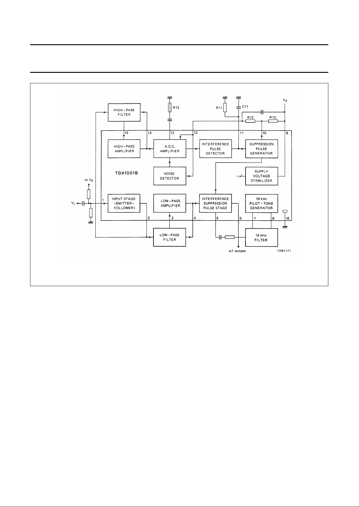
The TDA1001B is a monolithic integrated circuit for suppressing interference and noise in FM mono and stereo receivers.
Features
• Active low-pass and high-pass filters
• Interference pulse detector with adjustable and controllable response sensitivity
• Noise detector designed for FM i.f. amplifiers with ratio detectors or quadrature detectors
• Schmitt trigger for generating an interference suppression pulse
• Active pilot tone generation (19 kHz)
• Internal voltage stabilization
QUICK REFERENCE DATA
Supply voltage (pin 9) V
Supply current (pin 9) I
P
P
typ. 12 V
typ. 14 mA
A.F. input signal handling (pin 1)
(peak-to-peak value) V
Input resistance (pin 1) R
Voltage gain (V
1-16/V6-16
)G
i(p-p)
i
v
typ. 1 V
min. 35 kΩ
typ. 0,5 dB
Total harmonic distortion THD typ. 0,25 %
Bandwidth B typ. 70 kHz
Suppression pulse threshold voltage
(peak value); R
= 0 V
13
Suppression pulse duration t
Supply voltage range (pin 9) V
Operating ambient temperature range T
i(tr)OM
s
P
amb
typ. 19 mV
typ. 27 µs
7,5 to 16 V
−30 to + 80 °C
PACKAGE OUTLINE
TDA1001B: 16-lead DIL; plastic (SOT38); SOT38-1; 1996 September 06.
TDA1001BT: 16-lead mini-pack; plastic (SO16; SOT109A); SOT116-1; 1996 September 06.
December 1982 2
Philips Semiconductors Product specification
Interference and noise suppression circuit
for FM receivers
TDA1001B
TDA1001BT
Fig.1 Block diagram.
December 1982 3
Philips Semiconductors Product specification
Interference and noise suppression circuit
for FM receivers
TDA1001B
TDA1001BT
RATINGS
Limiting values in accordance with the Absolute Maximum System (IEC 134)
Supply voltage (pin 9) V
Input voltage (pin 1) V
Output current (pin 6) I
P
1-16
6
−I
6
max. 18 V
max. V
P
max. 1 mA
max. 15 mA
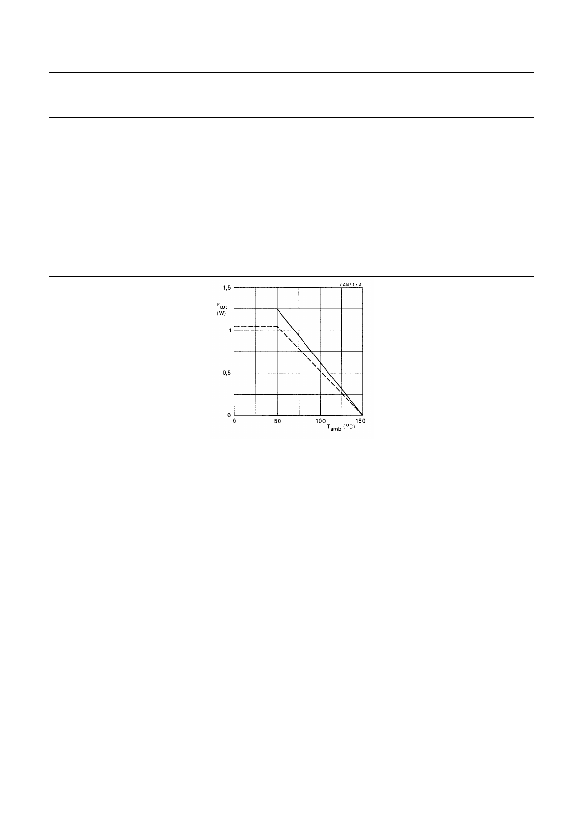
Total power dissipation see derating curves Fig.2
Storage temperature range T
Operating ambient temperature range T
stg
amb
−65 to +150 °C
−30 to +80 °C
V
in plastic DIL (SOT-38) package (TDA1001B).
− − − − − − in plastic mini-pack (SO-16; SOT-109A) package (TDA1001BT); mounted on a ceramic substrate of 50×15 ×0,7 mm.
Fig.2 Power derating curves.
December 1982 4
 Loading...