

Philips NE555, SA555, SE555, SE555C Technical data
Philips Semiconductors Linear Products Product specification
NE/SA/SE555/SE555CTimer
346
August 31, 1994 853-0036 13721
DESCRIPTION
The 555 monolithic timing circuit is a highly stable controller capable
of producing accurate time delays, or oscillation. In the time delay
mode of operation, the time is precisely controlled by one external
resistor and capacitor. For a stable operation as an oscillator, the
free running frequency and the duty cycle are both accurately
controlled with two external resistors and one capacitor. The circuit
may be triggered and reset on falling waveforms, and the output
structure can source or sink up to 200mA.
FEATURES
•Turn-off time less than 2µs
•Max. operating frequency greater than 500kHz
•Timing from microseconds to hours
•Operates in both astable and monostable modes
•High output current
•Adjustable duty cycle
•TTL compatible
•Temperature stability of 0.005% per °C
APPLICATIONS
•Precision timing
•Pulse generation
•Sequential timing
•Time delay generation
•Pulse width modulation
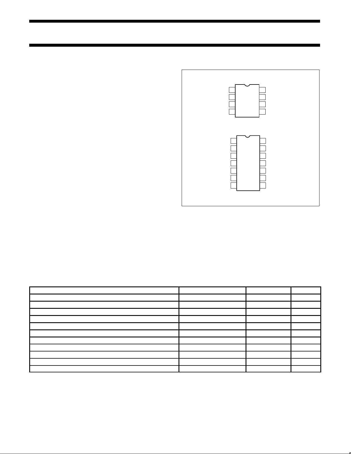
PIN CONFIGURATIONS
1
2
3
4 5
6
7
8
1
2
3
4
5
6
7 8
14
13
12
11
10
9
GND
TRIGGER
OUTPUT
RESET
GND
NC
TRIGGER
OUTPUT
NC
RESET
NC
DISCHARGE
THRESHOLD
CONTROL VOLTAGE
NC
DISCHARGE
NC
THRESHOLD
NC
CONTROL VOLTAGE
V
CC
V
CC
D, N, FE Packages
TOP VIEW
F Package
ORDERING INFORMATION
DESCRIPTION TEMPERATURE RANGE ORDER CODE DWG #
8-Pin Plastic Small Outline (SO) Package 0 to +70°C NE555D 0174C
8-Pin Plastic Dual In-Line Package (DIP) 0 to +70°C NE555N 0404B
8-Pin Plastic Dual In-Line Package (DIP) -40°C to +85°C SA555N 0404B
8-Pin Plastic Small Outline (SO) Package -40°C to +85°C SA555D 0174C
8-Pin Hermetic Ceramic Dual In-Line Package (CERDIP) -55°C to +125°C SE555CFE
8-Pin Plastic Dual In-Line Package (DIP) -55°C to +125°C SE555CN 0404B
14-Pin Plastic Dual In-Line Package (DIP) -55°C to +125°C SE555N 0405B
8-Pin Hermetic Cerdip -55°C to +125°C SE555FE
14-Pin Ceramic Dual In-Line Package (CERDIP) 0 to +70°C NE555F 0581B
14-Pin Ceramic Dual In-Line Package (CERDIP) -55°C to +125°C SE555F 0581B
14-Pin Ceramic Dual In-Line Package (CERDIP) -55°C to +125°C SE555CF 0581B
现货库存、技术资料、百科信息、热点资讯,精彩尽在鼎好!

Philips Semiconductors Linear Products Product specification
NE/SA/SE555/SE555CTimer
August 31, 1994
347
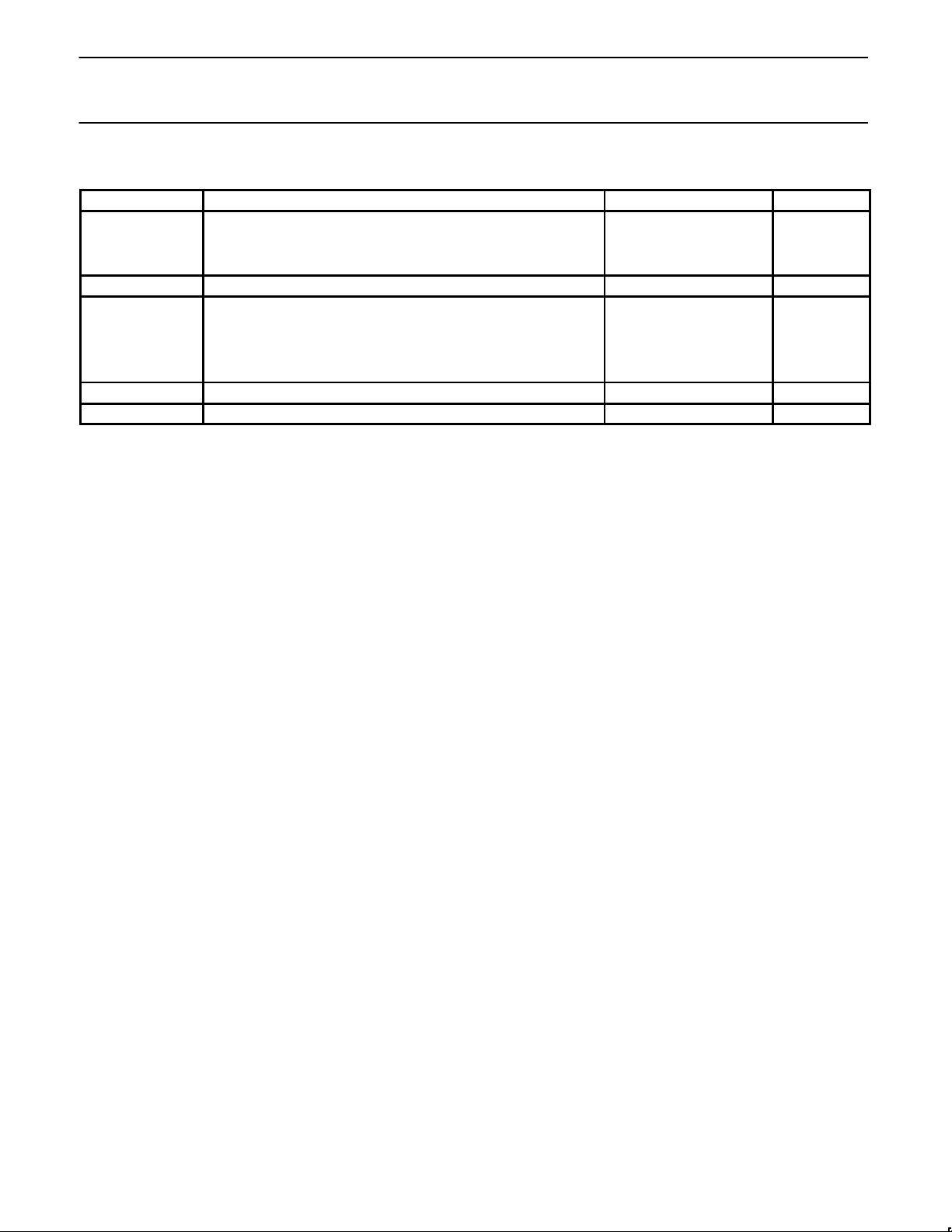
BLOCK DIAGRAM
COMPARATOR
COMPARATOR
FLIP FLOP
OUTPUT
STAGE
THRESH-
OLD
V
CC
6
7
3 1
4
2
5
8
R
R
R
CONTROL
VOLTAGE
TRIGGER
RESET
DIS-
CHARGE
OUTPUT GND
EQUIVALENT SCHEMATIC
NOTE: Pin numbers are for 8-Pin package
CONTROL VOLTAGE
FM
V
CC
R1
4.7K
R2
330
R3
4.7
K
R
4
1
K
R
7
5
K
R12
6.8K
Q21
Q9
Q8
Q7Q6
Q5
Q1
Q2 Q3
Q4
Q19
Q22
R13
3.9K
OUTPUT
Q23
C
B
R1
0
82.
K
R5
10
K
Q10
Q11 Q12
Q13
Q20
R11
4.7K
CB
Q18
E
R8
5K
Q17
Q16
Q15
R6
100K
R16
100
Q14
Q25
R9
5K
R15
4.7K
Q24
R14
220
THRESHOLD
TRIGGER
RESET
DISCHARGE
GND
Philips Semiconductors Linear Products Product specification
NE/SA/SE555/SE555CTimer
August 31, 1994
348
ABSOLUTE MAXIMUM RATINGS
SYMBOL PARAMETER RATING UNIT
Supply voltage
V
CC
SE555 +18 V
NE555, SE555C, SA555 +16 V
P
D
Maximum allowable power dissipation
1
600 mW
T
A
Operating ambient temperature range
NE555 0 to +70 °C
SA555 -40 to +85 °C
SE555, SE555C -55 to +125 °C
T
STG
Storage temperature range -65 to +150 °C
T
SOLD
Lead soldering temperature (10sec max) +300 °C
NOTES:
1. The junction temperature must be kept below 125°C for the D package and below 150°C for the FE, N and F packages. At ambient temperatures above 25°C, where this limit would be derated by the following factors:
D package 160°C/W
FE package 150°C/W
N package 100°C/W
F package 105°C/W
 Loading...