

Philips rc110an1 DATASHEETS

APPLICATION NOTE
Read/Write Devices based on the
HITAG Read/Write IC HTRC110
AN97070
December 1997 Revision 1.1

Philips Semiconductors
Read/Write Devices based on the HITAG
Read/Write IC HTRC110
Abstract
Designing read/write device (RWD) units for industrial RF-Identification applications is strongly facilitated by the
Philips HITAG Reader Chip HTRC110. All needed function blocks like antenna driver, modulator demodulator
and antenna diagnosis unit are integrated in the HTRC110. Therefore only a minimal number of additional passive components are required for a complete RWD.
This Application Note describes how to design an industrial RF-Identification system with the HTRC110. A major
focus is on dimensioning the antenna, all other external components including clock and power supply, as well as
on the demodulation principle and its imp lementation.
Application Note
AN97070
Philips Electronics N.V. 1997
All rights are reserved. Reproduction in whole or in part is prohibited without the prior written consent of the copyright owner.
The information presented in this document does not form p art of any quot ation or c ontract, is beli eved to be
accurate and reliable and may be changed without notice. No liability will be accepted by the publisher for any
consequence of its use. Publi cation th ereof does not convey nor i mply any l icense unde r patent- o r oth er industrial or intellectual property rights.
2

Philips Semiconductors
Read/Write Devices based on the HITAG
Read/Write IC HTRC110
APPLICATION NOTE
Read/Write Devices based on the
HITAG Read/Write IC HTRC110
AN97070
Author(s):
Thomas Giesler, Jörg Becker
Systems Laboratory Hamburg
Germany
Application Note
AN97070
Keywords
Basestation
Reader
HTRC110
HITAG
Antenna Design
RF-Identification
Date: 17. December 1997
3

Philips Semiconductors
Read/Write Devices based on the HITAG
Read/Write IC HTRC110
Summary
First, the fundamental external connections and supplies, as power and clock are described. The antenna design
and proper choice of the electrical antenna parameters are explained into depth. After this, the fundamental
demodulator principle and the idea behind the new Adaptive-Sampling-Time algorithm are described as well as
its practical implementation.This Application Note also covers the methods of writing data to the transponder and
shows special methods for fast demodulator settling. Also the fundamental methods for system performance and
tolerance measurements are presented.
All presented numeric parameters base on the HTRC110 HITAG Reader Chip data sheet; product specification;
Rev. 1.1 December 1997.
Application Note
AN97070
4

Philips Semiconductors
Read/Write Devices based on the HITAG
Read/Write IC HTRC110
Application Note
AN97070
CONTENTS
1. Introduction . . . . . . . . . . . . . . . . . . . . . . . . . . . . . . . . . . . . . . . . . . . . . . . . . 7
2. Power supply . . . . . . . . . . . . . . . . . . . . . . . . . . . . . . . . . . . . . . . . . . . . . . . . 8
2.1 Supply regulation, decoupling and ripple criteria . . . . . . . . . . . . . . . . . . . . . . . . . . . 8
2.2 Power-down modes . . . . . . . . . . . . . . . . . . . . . . . . . . . . . . . . . . . . . . . . . 8
2.2.1 Driver-off mode . . . . . . . . . . . . . . . . . . . . . . . . . . . . . . . . . . . . . . 8
2.2.2 Idle mode . . . . . . . . . . . . . . . . . . . . . . . . . . . . . . . . . . . . . . . . . 9
2.2.3 Power-down mode . . . . . . . . . . . . . . . . . . . . . . . . . . . . . . . . . . . . 9
3. External filtering capacitors . . . . . . . . . . . . . . . . . . . . . . . . . . . . . . . . . . . . . . . . 9
4. Clock . . . . . . . . . . . . . . . . . . . . . . . . . . . . . . . . . . . . . . . . . . . . . . . . . . . . . 9
5. MODE-pin . . . . . . . . . . . . . . . . . . . . . . . . . . . . . . . . . . . . . . . . . . . . . . . . . 10
6. Antenna design . . . . . . . . . . . . . . . . . . . . . . . . . . . . . . . . . . . . . . . . . . . . . . 11
6.1 Measuring the coupling factor . . . . . . . . . . . . . . . . . . . . . . . . . . . . . . . . . . . 11
6.2 Electrical antenna parameters . . . . . . . . . . . . . . . . . . . . . . . . . . . . . . . . . . . 12
6.2.1 Minimum antenna circuitry . . . . . . . . . . . . . . . . . . . . . . . . . . . . . . . 12
6.2.2 Antenna circuitry with driver short circuit protection. . . . . . . . . . . . . . . . . . . 12
6.2.3 Adding additional EMI-immunity to the system . . . . . . . . . . . . . . . . . . . . . 13
6.2.4 Dimensioning of the antenna components . . . . . . . . . . . . . . . . . . . . . . . 14
Antenna current adapting resistor. . . . . . . . . . . . . . . . . . . . . . . . . . . . 14
Antenna quality factor . . . . . . . . . . . . . . . . . . . . . . . . . . . . . . . . . . 15
Antenna inductance . . . . . . . . . . . . . . . . . . . . . . . . . . . . . . . . . . . 15
Antenna Capacitance . . . . . . . . . . . . . . . . . . . . . . . . . . . . . . . . . . 16
Optimizing the demodulator input resistor . . . . . . . . . . . . . . . . . . . . . . . 16
7. Antenna tuning . . . . . . . . . . . . . . . . . . . . . . . . . . . . . . . . . . . . . . . . . . . . . . 17
7.1 Tuning with a network analyzer. . . . . . . . . . . . . . . . . . . . . . . . . . . . . . . . . . . 17
7.2 In-system tuning . . . . . . . . . . . . . . . . . . . . . . . . . . . . . . . . . . . . . . . . . . 17
8. Antenna Diagnosis . . . . . . . . . . . . . . . . . . . . . . . . . . . . . . . . . . . . . . . . . . . . 17
8.1 Antenna fail detection. . . . . . . . . . . . . . . . . . . . . . . . . . . . . . . . . . . . . . . . 17
8.2 Antenna detuning detection . . . . . . . . . . . . . . . . . . . . . . . . . . . . . . . . . . . . 18
9. Reading data from the transponder . . . . . . . . . . . . . . . . . . . . . . . . . . . . . . . . . . . 18
9.1 Theoretical background. . . . . . . . . . . . . . . . . . . . . . . . . . . . . . . . . . . . . . . 18
9.1.1 Sampling demodulator principle. . . . . . . . . . . . . . . . . . . . . . . . . . . . . 21
9.1.2 Adaptive-Sampling-Time (AST) principle . . . . . . . . . . . . . . . . . . . . . . . . 24
9.2 Implementation of the AST-method employing the HTRC110 . . . . . . . . . . . . . . . . . . . 25
9.2.1 Phase shift measurement system. . . . . . . . . . . . . . . . . . . . . . . . . . . . 26
9.2.2 Calculating and setting the sampling time . . . . . . . . . . . . . . . . . . . . . . . 27
9.2.3 Software Implementation . . . . . . . . . . . . . . . . . . . . . . . . . . . . . . . . 27
9.2.4 Determining the offset compensation constant for a specific system. . . . . . . . . . 28
Typical values. . . . . . . . . . . . . . . . . . . . . . . . . . . . . . . . . . . . . . 28
Exact determination of the offset compensation constant . . . . . . . . . . . . . . . 28
9.3 Additional safety backup for defect transponders or RWD antennas. . . . . . . . . . . . . . . . 29
9.4 Monitoring the analog demodulator output signal . . . . . . . . . . . . . . . . . . . . . . . . . 29
9.5 Adapting the demodulator to different transponders and applications by register settings. . . . . 30
5

Philips Semiconductors
Read/Write Devices based on the HITAG
Read/Write IC HTRC110
9.5.1 Demodulator bandwidth. . . . . . . . . . . . . . . . . . . . . . . . . . . . . . . . . 30
9.5.2 Demodulator gain . . . . . . . . . . . . . . . . . . . . . . . . . . . . . . . . . . . . 30
9.5.3 Digitizer hysteresis . . . . . . . . . . . . . . . . . . . . . . . . . . . . . . . . . . . 31
9.6 Reading out the digital data . . . . . . . . . . . . . . . . . . . . . . . . . . . . . . . . . . . . 31
10. Sending data to the transponder . . . . . . . . . . . . . . . . . . . . . . . . . . . . . . . . . . . . . 31
10.1 Modulation principle . . . . . . . . . . . . . . . . . . . . . . . . . . . . . . . . . . . . . . . . 31
10.2 Driver-off period width and position. . . . . . . . . . . . . . . . . . . . . . . . . . . . . . . . . 32
10.3 Sending data via the digital interface . . . . . . . . . . . . . . . . . . . . . . . . . . . . . . . . 32
11. Settling . . . . . . . . . . . . . . . . . . . . . . . . . . . . . . . . . . . . . . . . . . . . . . . . . . . 33
11.1 Oscillator settling . . . . . . . . . . . . . . . . . . . . . . . . . . . . . . . . . . . . . . . . . . 33
11.2 Field settling . . . . . . . . . . . . . . . . . . . . . . . . . . . . . . . . . . . . . . . . . . . . 33
11.3 Demodulator settling . . . . . . . . . . . . . . . . . . . . . . . . . . . . . . . . . . . . . . . . 33
11.4 General fast settling sequence . . . . . . . . . . . . . . . . . . . . . . . . . . . . . . . . . . . 34
11.5 After-WRITE fast settling sequence . . . . . . . . . . . . . . . . . . . . . . . . . . . . . . . . 34
12. Power-on sequence . . . . . . . . . . . . . . . . . . . . . . . . . . . . . . . . . . . . . . . . . . . . 35
13. Tolerance field verification . . . . . . . . . . . . . . . . . . . . . . . . . . . . . . . . . . . . . . . . 35
13.1 Tolerance field measurement setup . . . . . . . . . . . . . . . . . . . . . . . . . . . . . . . . 35
13.2 Tolerance field matrix measurement . . . . . . . . . . . . . . . . . . . . . . . . . . . . . . . . 37
Application Note
AN97070
14. References. . . . . . . . . . . . . . . . . . . . . . . . . . . . . . . . . . . . . . . . . . . . . . . . . 38
6
Philips Semiconductors
Read/Write Devices based on the HITAG
Read/Write IC HTRC110
Application Note
AN97070
1. Introduction
With the HITAG Reader Chip, H TRC110 a highl y integra ted RWD with a powerful circuit implementation is avai lable.
The HTRC110 is ideally suite d to design an advanced RWD for industrial applications. The device in corporates
all necessary functions to facilitate reading and writing to an external transponder.
It makes use of a unique demodulation technique that extends the system operation range compared with first
generation envelope detection based systems.
The HTRC110 is optimized to operate with the Philips transponder family HITAG1 & 2.
Device characteristics like receiver gain and bandwidth or transmit timing are widely programmable, in order to
match the RWD to the used transponder.
The HTRC110 has been designed to fit for ’Intelligent Antenna’ as well as for ’Active Antenna’ applications.
For the purpose of system diagnostics, the HTRC110 provides antenna failure detection.
Designed for low power consumption employing CMOS technology, the device supports IDLE and POWER-
DOWN modes.
The HTRC110 requires only very view external components and comes in a SO14 plastic package.
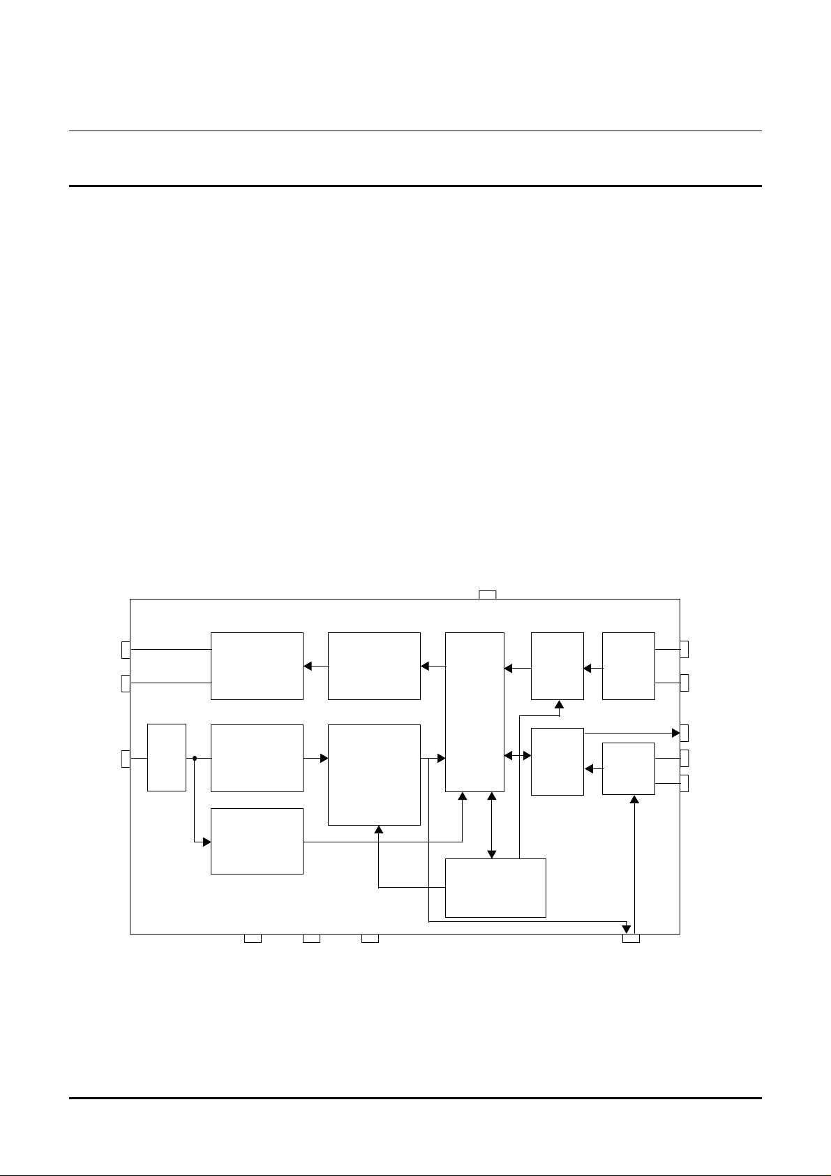
TX1
TX2
RX
EMI
filter
antenna drivers
demodulator
phase
measurement
QGND CEXT VSS
bandpass filter
amplifier
dynamic control
digitizer
modulator
VDD
control
unit
control registers
programmable
divider
serial
interface
oscillator
digital
glitch
filters
MODE
XTAL1
XTAL2
DOUT
DIN
SCLK
Fig.1 HTRC110 block diagram
7

Philips Semiconductors
Read/Write Devices based on the HITAG
Read/Write IC HTRC110
Application Note
AN97070
2. Power supply
The supply current of the HTRC110 consists of two components:
- 10 mA
- the current driven into the antenna resonance circuit
As the antenna current is nearly sine shaped, the average DC-current component can be calculated by:
I
ant
DC
where Î
results in 10 mA + 2/π * 200 mA = 137 mA. Using the burst mode, where Î
at a pulse/pause ratio of 1:4, I
When switching on the power supply, the HTRC110 performs an internal power-on reset, where all internal registers (e.g. the configuration pages) are reset to their initial settings (see [1]).
2.1 Supply regulation, decoupling and ripple criteria
Any supply voltage fluctuations or ripple are transferred into antenna current fluctuations by the antenna driver
transistors. This is equal to a current modulation that results in a voltage modulation at the antenna tap point.
There is no possibility for the demodula tor to distinguish this modulation from the transponder modulation. Especially in the passband of the demodulator filters, the system is very sensitive against supply hum and ripple.
maximum for the supply of the IC with its internal function blocks
DC
2
ˆ
-- -
I
=
ant
π
describes the antenna current amplitude. With Î
ant
= 265 mA respectively.
antDC
= 200 mA the maximum overall supply current
ant
= 400 mA is allowed for ton < 400 ms
ant
Therefore, supply fluctuations cause strong signal disturbances at the demodulator output. Because of this,
selecting a proper stable supply regulator is essential for good system performance.
Also the power supply should be de coupled via a 10µ F capaci tor in parallel to a 100nF capac itor. It is recommended to choose SMD- compo nent s bein g pl aced d irectl y betwee n the VDD- and VSS-pins (Pin-Nr. 1 and 3) in
the immediate vicinity of the H TRC110 .
2.2 Power-down modes
Three different po wer-down mo des have been implement ed in the HTR C110 for ene rgy saving du ring times ,
where the RWD functionality is not needed
After switching back to normal operation mode fr o m all of these three PD modes, it is essenti al to inv o ke the settling procedure described in section 11. to allow for a fast filter and threshold settling. Without this procedure, settling (being not ready for transponder data) may require several ten milliseconds.
2.2.1 Driver-off mode
By setting the TXDIS bi t, the antenn a driver s can be switched off. All remaining circuit ries of the HTRC11 0 stay
active. Driver-off mode is activated by setting the following bit combinati on vi a SET_CONFIG_PA GE_1 :
PD_MODE = don’t care
PD = 0
TXDIS = 1
The other bits in the configuration page 1 don’t affect this mode. The drivers are reactivated by resetting the
TXDIS bit.
8

Philips Semiconductors
Read/Write Devices based on the HITAG
Read/Write IC HTRC110
Application Note
AN97070
2.2.2 Idle mode
In some applications, the HTRC110 oscillator is used to clo c k the microprocessor. In this case , the oscill ator has
still to run while the rest of the HTRC110 functionality is powered down. For this purpose, the so called idle mode
has been implemented. The idle mode is entered by setting the follo win g bit co mbination:
PD_MODE = 0
PD = 1
TXDIS = don’t care
Resetting the PD-bit leaves the idle mode.
2.2.3 Power-down mode
It is possible to switch off the whole IC (except the serial inter face) by putting it into the power-dow n mode. The
power-down mode can be activated by the following settings:
PD_MODE = 1
PD = 1
TXDIS = don’t care
Resetting the PD-bit leaves the power-down mode.
3. External filtering capacitors
For bypassing the internal analog virtual ground (~2V), a 100nF capacit or has to be conne cted fro m the QGNDpin to the VSS-pin. This capacitor connection should be low impedance and close to the IC.
Another 100nF capacitor is connected from CEXT to VSS which is needed for the 2nd high pass filter. Both
capacitors can be ordinary ceramic capacitors.
Leakage currents into CEX T, e.g. caused b y dirt or humidity on th e PCB, can cause o ffsets in the dem odulator
reducing the sensitivity. Therefore it is recommended to place a guar d ring at the Q GND potentia l around the
CEXT-pin - capacitor lead. The implementation of this guard ring is facilitated because the QGND- and CEXTpins are next to each other and pin 11 is not connected.
4. Clock
The HTRC110 contains an internal clock oscillator being capable to operate with an external quartz or ceramic
resonator for frequency stabilization. It is also possib le to use this oscillator for cloc king a connected microcontroller. Further, the HTRC110 can be clocked by e.g. a microcontroller (Fig.2).
HTRC110
in out
XTAL1 XTAL2
µC
in out in out
XTAL1 XTAL2
HTRC110
XTAL1 XTAL2
µC
in out in out in out
XTAL1 XTAL2
HTRC110
XTAL1 XTAL2
µC
XTAL1 XTAL2
Fig.2 HTRC110 Clock
9

Philips Semiconductors
Read/Write Devices based on the HITAG
Read/Write IC HTRC110
The internal oscillator is well suited for standard parallel resonance quartz crystals. The capacitors to VSS should
be chosen according to the quartz manufacturer specification.
With ceramic resonators, the capacitors are often included internally in the resonator package. Ce ramic resonators have a higher tolerance than quartz crystals (e.g. 0.5%). This tolerance adds to the resonance frequency tolerances of the RWD antenna as well as on the transponder tolerance. That means a system frequency shift
caused by oscillator tolerances causes a relative shift versus transpond er and R WD centre frequency. Systems
with relatively high coupl ing fact or and hi gh fi eld strengt h at th e tran spond er locatio n natural ly h ave a la rge sa fe
operation tolerance are a. In this cases th e additio nal transpond er os cillat or toleran ce d oes not cause p roble ms.
In more critical systems, where the safe operati ng area regard ing frequency tolerance is small be cause o f a lo w
coupling factor or a low field strength at the transponder, we recommend to use a quartz crystal.
In applications, where the HTRC110 is mounted together with the µC on the same PCB, only one clock oscillator
is needed, re sulti ng in sa ving e .g. on e qu art z cry st al whi ch is a r el ativ ely exp ensiv e co mpon ent. Th e H TRC1 10
oscillator output XTAL2 can be directl y connected to most microcontroll er clock inputs. It is also possible to use
the microcontroller oscillator to clock the HTRC110 via XTAL1.
Jitter on the HTRC110 clo ck is trans ferred directl y into demod ulator noi se depend ing on the sampling ph ase.
Therefore, supplying the HTRC110 with an external high jitter oscillator may reduce system performance. S pec ial
care has been taken at the in ternal H TRC110 oscil lator de sign to avoi d jitter and also to gu arantee a fast power
on oscillator settling. Therefore, if there are doubts about the quality of the µC-oscillator, it’s a good idea to supply
the µC with the HTRC110 clock.
Application Note
AN97070
When supplying the µC with the HTRC110 clock, it is important not to use the power-down mode, because in this
case the oscillator is switched off, also stopping the µC. The idle mode is recommended for that case.
Hum picked up by electromagnetic interference (EMI) or capa citive feed through on the PCB into the cl ock connection between HTRC110 and µC can also cause clock jitter. Therefore a short leads length of this interconnection is recommended.
The HTRC110 oscillat or wo rks toge ther w ith 4, 8, 12 an d 16 MHz q uartz cryst als. Also extern al clo ck sign als at
the same frequencies can be supplied into XTAL1. The system frequency o f 125kHz is ge nerate d inte rn al ly fr o m
this clock via a software programmable frequency divider.
The division factor should be set du ring the H TRC110 initial ization phase a fter power-up by con figuring the bi ts
FSEL0 and FSEL1 if the clock frequency is different to the initi al value of 4 MHz. This is done via the co mmand
SET_CONFIG_PAGE 3. E.g. adjusting to a clock frequency of 12 MHz is done by the command:
SET_CONFIG_PAGE 3, xx10b
5. MODE-pin
MODE is a multi-function pin. In normal operation, it is used for switching on and o ff the internal digital g litch filters on DIN and SCLK.
If MODE is permanently connected to VSS, the glitch filters are in off-state and the serial interface can be used at
high data rates only limited by the specified setup and hold times.
Connecting MODE permanently to VDD activates the internal glitch fil ters. This mode should only be used if the
HTRC110 serial interface is connected via a rel atively long lead to the µC where EMI-pro blems may occur. The
glitch filters limit the data transfer rate. A more detai led description of the glitch fil ter usage will be provided in
future. Currently we recommend the glitch filter “off”-configuration.
In a special configuration, during system development, MODE can also be configured to output the demodulated
signal after amplification and filtering (see section 9.4).
10

Philips Semiconductors
Read/Write Devices based on the HITAG
Read/Write IC HTRC110
Application Note
AN97070
6. Antenna design
Most important for a good system pe rformance and large safety margins in wirele ss id entifi cation appli catio ns is
a proper design of the antenna. This means a good mechanical design for achieving a long operation distance
and a high coupling factor as well as the proper dimensioning of the electrical parameters of the antenna components.
The RWD antenna consist s of a RLC series re sonance circuit ry. The antenn a coil can be e.g. eit her circular or
rectangular shaped. The co il dimension depends on the applic ation, espec ially on the requir ed operation dis tance. The major boundary conditions for the antenna design are:
- the maximum antenna current provided by the RWD antenna drivers
- the maximum quality factor related to the required data bandwidth
- the maximum antenna inductance resulting from the antenna current and the quality factor
- the minimum operation field strength of the applied transponder
- the minimum coupling factor required for properly demodulating the data sent to the RWD
- the antenna diameter or size
Small antenna coils provide a high field strength and coupling factor, when the transponder is positioned rela-
tively close to the antenna. Bot h, the field st rength and co upling fact or show a strong decay when the transpo nder distance is increased. Therefore, small antennas are well suited for short range applications.
Large antenna coils operated at the s a me antenna current produce a lo wer ze ro distance fiel d stren gth an d coupling factor, but also the field strength is decaying much slower with increased distance.
For circular antenna coils it can be shown mathematically, that with a given maximum antenna current Î
maximum inductance L
ˆ
B
the optimum antenna radius r
min
(resulting from the maximum Q) and minimum transponder operating field strength
amax
achieving the maximum distance not dropping below is roughly given
opt
ˆ
B
min
antmax
by:
0
µH
------- -
for a ’short cylinder coil’,≅
m
4π 10
⋅=
7–
Vs
-------- -
Am
r
opt
L
max
------------ -
≅
3
c
ˆ
I
max
min
2
µ
0
----------------- -
⋅
ˆ
B
c26
µ
It can be further shown, that the herewith achieved distance from the antenna plane to the transponder on the
coil centre axis equals the optimized coil radius r
opt
.
The optimisation which was discussed so far conside red only the tag´s po wer requirements and supply. If the
operation distance is limited by the data transmission channel, a smaller antenna radius may give better results.
6.1 Measuring the coupling factor
The coupling factor k describes how close the R WD antenna and the transponder anten na are coupled to each
other or, in other words, “how many field lines of the RWD antenna are captured by the transponder antenna”.
The coupling factor is a purely geometric p arameter bei ng independ ent from th e antenna i nductance s. It only
depends on the form and size of the antennas, thei r placement relative to ea ch oth er a nd t he materials inside or
close to the coils.
,
The coupling factor is one of the most important parameters considering the system performance, tolerance
ranges and signal to noise ratio. The relat ion betwe en coupling fa ctor and syste m performance is stronger t han
linear.
11

Philips Semiconductors
Read/Write Devices based on the HITAG
Read/Write IC HTRC110
Application Note
AN97070
To measure the coupling factor, a transponder coil without the transponder chip is needed fro m the transponder
manufacturer. This transp onder coil is placed instead of the transpo nde r into the antenn a field. The antenna co il
is excited permanently at 125 kHz by the HTRC110-RWD or by a 125 kHz sine wave frequency generator.
The voltage across the antenna coil and the transponde r coi l shoul d be me asured via high imp edan ce probes or
by a proper volt-meter, that is capable to handle 125 kHz correctly. It is important not to apply high resistive or
capacitive loads to the relatively high impedance transponder coil by the measurement equipment for measuring
the real open circuit voltage. If the HTRC110 is used for exciting the antenna, potential-free s copes or meters
should be used because of the full bridge drivers. Alternatively the voltage from the antenna tap point (coil-capacitor connection) can be measured again st ground via an ordinary scope or meter.
The coupling factor k results from:
U
transponder coil
-------------------------------------------- -
k
U
antenna
L
antenna
------------------------------------------- -=
L
transponder coil
6.2 Electrical antenna parameters
The following secti ons des cribe m ethods f or calcula ting the proper el ectrical antenna parame ters as ante nna
inductance, resistance and capacitance.
6.2.1 Minimum antenna circuitry
The minimum antenna circuitry applicable for the HTRC110 is depicted in Fig.3.
TX1
R
a
L
a
C
a
TX2
tap point
R
v
Fig.3 Minimum antenna circuitry
RX
Normally Ra is needed to adapt the antenna quality factor and by this adapt the maximum antenna current.
6.2.2 Antenna circuitry with driver short circuit protection
In applications, where the HTRC110 and the antenna coil together form a closed module, the so called ac tive
antenna applications, short circuit protection of the driver pins is normally not required. In other applications, were
the HTRC110 and th e antenna coil are sepa rated and con nected to ea ch other vi a a cable, sho rt circuit protec tion against VDD and VS S may be requi red. This can b e achi ev ed for bo th driver pins by dividin g the resonan ce
capacitor into two components (C
and Cs) as shown in Fig.4.
a
12
 Loading...