Philips rc110 DATASHEETS

INTEGRATED CIRCUITS
HTRC110
Hitag Reader Chip
Product Specification (Rev. 1.1)
December 1997

Philips Semiconductors Product Specification
Hitag Reader Chip HTRC110
CONTENTS
1 FEATURES
2 GENERAL DESCRIPTION
3 ORDERING INFORMATION
4 BLOCK DIAGRAM
5 KEY DATA
6 PINNING INFORMATION
6.1 Pinning Diagram
6.2 Pin Description
7 MINIMUM APPLICATI ON CIRCUI TRY
8 FUNCTIONAL DESCRIPT ION
8.1 Power Supply
8.2 Antenna Drivers, Data Input
8.3 Diagnosis
8.4 Oscillator / Programmable Divider / Clock
8.5 Adaptive Sampling Time Demodulator
8.6 Idle and Power-down Mode
8.7 Serial Interface
8.7.1 Glitch Filter for Increased Noise/Interference Imm unity
9 COMMANDS
9.1 READ_TAG
9.2 WRITE_TAG_N
9.3 WRITE_TAG
9.4 READ_PHASE
9.5 SET_SAMPLING_TI ME
9.6 GET_SAMPLING_TIME
9.7 SET_CONFIG_PAG E
9.8 GET_CONFIG_PAGE
10 ABSOLUTE MAXIMUM RATINGS
11 DC CHARACTERISTICS
12 AC CHARACTERISTICS
13 PACKAGE
14 DEFINITIONS
15 LIFE SUPPORT APPLICATIONS
Rev. 1.1 2

Philips Semiconductors Product Specification
Hitag Reader Chip HTRC110
1 FEATURES
Combines all analogue RFID reader hardware in a single
chip
· Optimized for HITAG transponder family
· Robust antenna coil power driver stage with modulator
· High performance adaptive sampling time AM/PM
demodulator (patent pending)
· Read and write function
· On-chip clock oscillator
· Antenna rupture and short circuit detection
· Low power consumption
· Very low power stand-by mode
· Low external component count
· Small package (SO14)
2 GENERAL DESCRIPTION
The Hitag Reader Chip HTRC110 is intended for use
with transponders which are based on the HITAG silicon (HT1ICS30 02x or HT2ICS20 02x). (E.g. the
HITAG 2 stick HT2DC20 S20 may be operated with the
use of the Reader Chip). In addition the IC supports
other 125kHz transponder types using amplitude modulation for the write operation and AM/PM for the read
operation. The receiver parameters (gain factors, filter
cutoff frequencies) can be optimized to system and
transponder requirements. The HTRC110 is designed
for easy integration into RF-identification readers.
State-of-the-art technology a llows alm ost c omplete integration of the necessary building blocks. A powerful
antenna driver/modulator together with a low-noise
adaptive sampling time demodulator, programmable filters/amplifier and digitizer build the complete transceiver unit, required to design high-performance
readers. A three-pin microcontroller interface is
employed for programming the HTRC110 as well as for
the bidirectional communication with the transponders.
The three-wire interface can be changed into a
two-wire interface by connecting the data input and the
data output.
Tolerance dependent zero amplitude modulation
caused severe problems in envelope detector systems,
resulting in the need of very low tolerance reader antennas. These problems are solved by the new Adaptive
Sampling Time technique (AST).
3 ORDERING INFORMATION
TYPE NAME DESCRIPTION ORDERING NUMBER
HTRC110 01T/02EE Hitag Reader IC, Tube 9352 600 91112
HTRC110 01T/03EE Hitag Reader IC, Reel 9352 600 92118
Rev. 1.1 3

Philips Semiconductors Product Specification
Hitag Reader Chip HTRC110
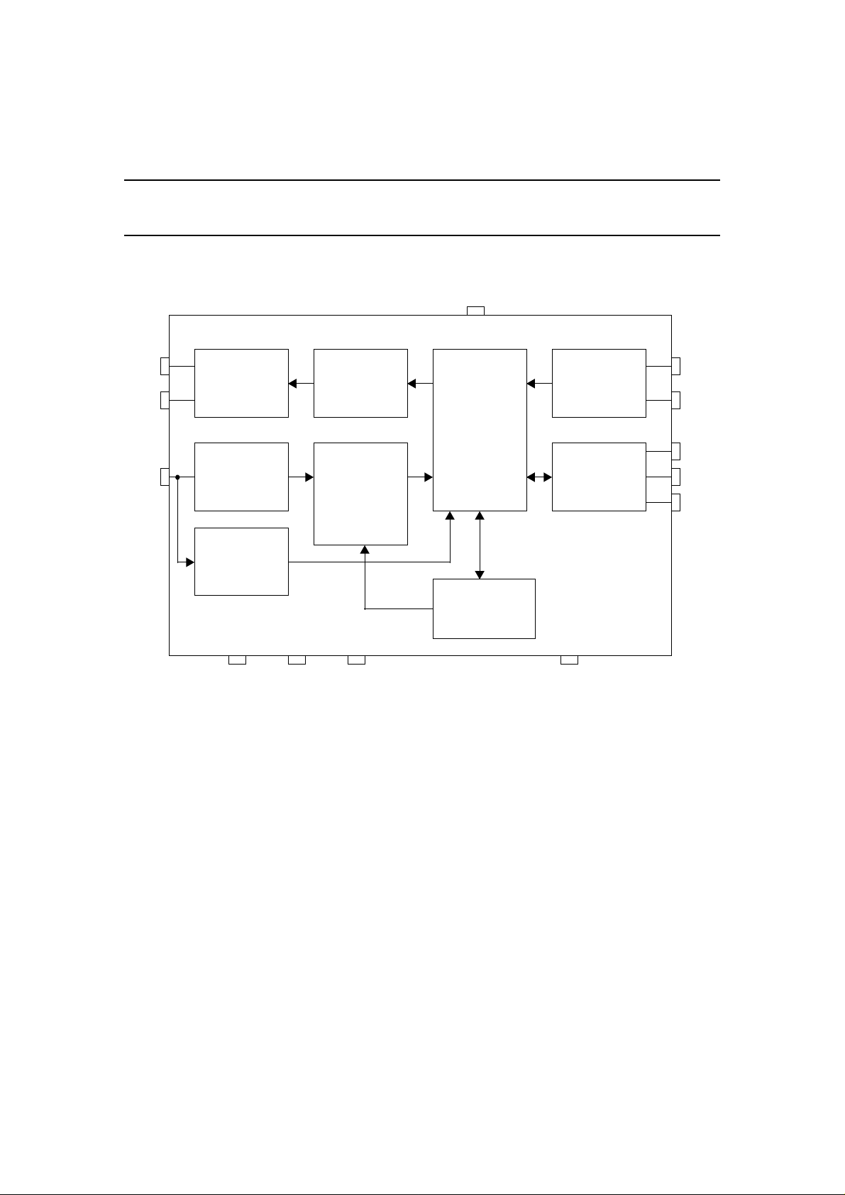
4 BLOCK DIAGRAM
VDD
TX1
TX2
RX
5 KEY DATA
Antenna Drivers Modulator
Synchron
Demodulator
Phase
Measurement
QGND CEXT
Bandpass Filter
Amplifier
Dynamic Control
Digitizer
VSS
Fig.1 Block diagram Hitag Reader Chip HTRC110
Control
Unit
Control Register
Oscillator
Serial Interface
MODE
XTAL1
XTAL2
DIN
DOUT
SCLK
Supply VDD 5 V ±10%
Clock/Osc. frequency 4,8,12,16 MHz programmable
(antenna carrier frequency 125 kHz)
Antenna driver current 200 mAp continuous
Serial interface CMOS compatible
Package SO14
Operation temperature range -40°C to +85°C
Rev. 1.1 4

Philips Semiconductors Product Specification
Hitag Reader Chip HTRC110
6 PINNING INFORMATION
6.1 Pinning Diagram
6.2 Pin Description
Number Symbol Description
1 VSS GND, negative supply input
2 TX2 Coil driver output
3 VDD Stabilized 5 V supply input
4 TX1 Coil driver output
5 MODE To enable filtering of SCLK and DIN (for active antenna applications)
6 XTAL1 Oscillator interface, input
7 XTAL2 Oscillator interface, output
8 SCLK Microcontroller interface: serial clock input
9 DIN Microcontroller interface: serial data in
10 DOUT Microcontroller interface: serial data out
11 n.c. Not connected
12 CEXT High pass filter coupling
13 QGND Analog ground bias
14 RX Demodulator input
Rev. 1.1 5

Philips Semiconductors Product Specification
Hitag Reader Chip HTRC110
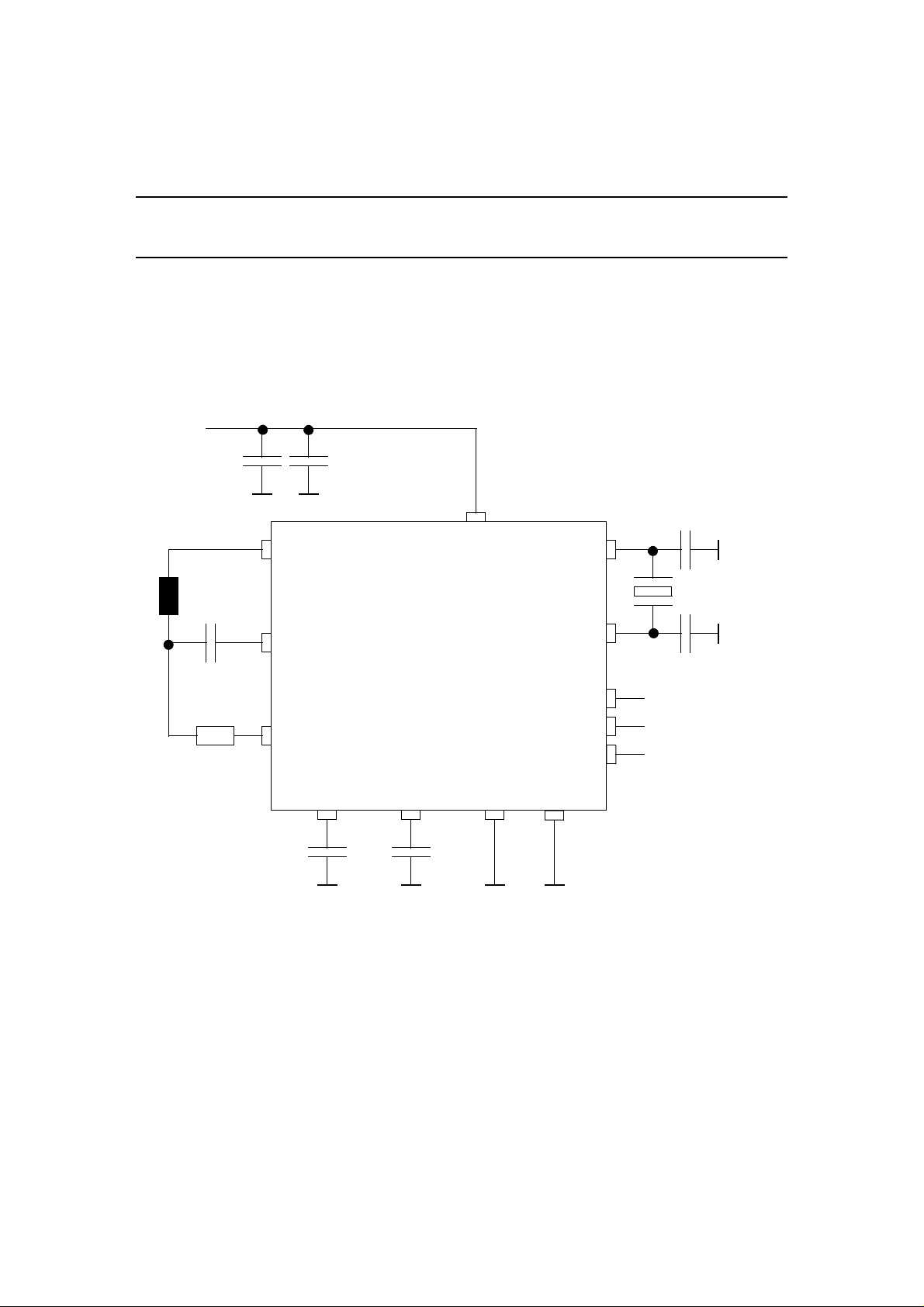
7 MINIMUM APPLICATIO N CIRCUI TRY
The following figure shows a minimal application circuitry for the HTRC110. The reader coil L
together with the
a
capacitor Ca forms a series resonant LC circuit (f = 125 kHz). The high voltages in the LC circuit are divided to safe
operating levels by R
and the chip internal resistor R
v
behind the RX-pin. The two capacitors connected to
dem_in
XTAL1 and XTAL2 shall be the recommended values and types from th e crystal’s dat a sheet. Alte rnatively to a crys tal a ceramic resonator can be used or an external clock source can be connected to XTAL1.
VDD
+
L
10µF
a
TX1
C
a
TX2
100nF
VDD
XTAL1
XTAL2
DIN
R
v
RX
DOUT
SCLK
TO
MICROPROCESSOR
QGND
CEXT VSS
MODE
100nF100nF
Fig.2 Minimum application circuitry
Rev. 1.1 6
 Loading...